- You are here:
-
Home

-
Contents
-
Part XIII. Manufacturing Industries
- Microelectronics and Semiconductors

83. Microelectronics and Semiconductors
Chapter Editor: Michael E. Williams
Table of Contents
Tables and Figures
General Profile
Michael E. Williams
Silicon Semiconductor Manufacturing
David G. Baldwin, James R. Rubin and Afsaneh Gerami
Liquid Crystal Displays
David G. Baldwin, James R. Rubin and Afsaneh Gerami
III-V Semiconductor Manufacturing
David G. Baldwin, Afsaneh Gerami and James R. Rubin
Printed Circuit Board and Computer Assembly
Michael E. Williams
Health Effects and Disease Patterns
Donald V. Lassiter
Environmental and Public Health Issues
Corky Chew
Tables
Click a link below to view table in article context.
1. Photoresist systems
2. Photoresist strippers
3. Wet chemical etchants
4. Plasma etching gases & etched materials
5. Junction formation dopants for diffusion
6. Major categories of silicon epitaxy
7. Major categories of CVD
8. Cleaning of flat panel displays
9. PWB process: Environmental, health & safety
10. PWB waste generation & controls
11. PCB waste generation & controls
12. Waste generation & controls
13. Matrix of priority needs
Figures
Point to a thumbnail to see figure caption, click to see figure in article context.
|
|


General Profile
The diversity of processes and products within the microelectronics and semiconductor industry is immense. The focus of the occupational health and safety discussion in this chapter centres on semiconductor integrated circuit (IC) production (both in silicon-based products and valence III-V compounds), printed wiring board (PWB) production, printed circuit board (PCB) assembly and computer assembly.
The industry is composed of numerous major segments. The Electronics Industry Association uses the following delineation in reporting data on pertinent trends, sales and employment within the industry:
- electronic components
- consumer electronics
- telecommunications
- defence communications
- computers and peripheral equipment
- industrial electronics
- medical electronics.
Electronic components include electron tubes (e.g., receiving, special-purpose and television tubes), solid-state products (e.g., transistors, diodes, ICs, light-emitting diodes (LEDs) and liquid-crystal displays (LCDs)) and passive and other components (e.g., capacitors, resistors, coils, transformers and switches).
Consumer electronics include television sets and other home and portable audio and video products, as well as information equipment such as personal computers, facsimile transmission machines and telephone answering devices. Electronic gaming hardware and software, home security systems, blank audio and video cassettes and floppy disks, electronic accessories and total primary batteries also fall under the consumer electronics heading.
In addition to general purpose and specialized computers, computers and peripheral equipment includes auxiliary storage equipment, input/output equipment (e.g., keyboards, mice, optical scanning devices and printers), terminals and so on. While telecommunications, defence communications and industrial and medical electronics utilize some of the same technology these segments also involve specialized equipment.
The emergence of the microelectronics industry has had a profound impact on the evolution and structure of the world’s economy. The pace of change within industrialized nations of the world has been greatly influenced by advances within this industry, specifically in the evolution of the integrated circuit. This pace of change is graphically represented in the timeline of the number of transistors per integrated circuit chip (see figure 1).
Figure 1. Transistors per integrated circuit chip

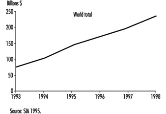
The economic importance of worldwide semiconductor sales is significant. Figure 2 is a projection by the Semiconductor Industry Association for worldwide and regional semiconductor sales for 1993 to 1998.
Figure 2. Worldwide semiconductor sales forecast
The semiconductor IC and computer/electronics assembly industries are unique compared to most other industrial categories in the relative composition of their production workforces. The semiconductor fabrication area has a high percentage of female operators that run the process equipment. The operator-related tasks typically do not require heavy lifting or excess physical strength. Also, many of the job tasks involve fine motor skills and attention to detail. Male workers predominate in the maintenance-related tasks, engineering functions and management. A similar composition is found in the computer/electronics assembly portion of this industry segment. Another unusual feature of this industry is the concentration of manufacturing in the Asia/Pacific area of the world. This is especially true in the final assembly or back-end processes in the semiconductor industry. This processing involves the positioning and placement of the fabricated integrated circuit chip (technically known as a die) on a chip carrier and lead frame. This processing requires precise positioning of the chip, typically through a microscope, and very fine motor skills. Again, female workers predominate this part of the process, with the majority of worldwide production being concentrated in the Pacific Rim, with high concentrations in Taiwan, Malaysia, Thailand, Indonesia and the Philippines, and growing numbers in China and Vietnam.
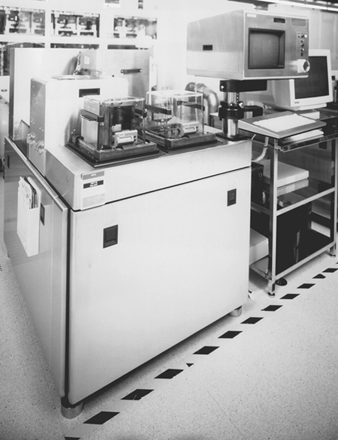
The semiconductor IC fabrication areas have various unusual properties and characteristics unique to this industry. Namely, the IC processing involves extremely tight particulate control regimens and requirements. A typical modern IC fabrication area may be rated as a Class 1 or less cleanroom. As a method of comparison, an outdoor environment would be greater than Class 500,000; a typical room in a house approximately Class 100,000; and a semiconductor back-end assembly area approximately Class 10,000. To attain this level of particulate control involves actually putting the fabrication worker in totally enclosed bunny suits that have air supply and filtration systems to control the levels of particulates generated by the workers in the fabrication area. The human occupants of the fabrication areas are considered very potent generators of fine particulates from their exhaled air, shedding of skin and hair, and from their clothing and shoes. This requirement for wearing confining clothing and isolating work routines has contributed to employees feeling like they are working in a “non-hospitable” work environment. See figure 3. Also, in the photolithographic area, the processing involves exposing the wafer to a photoactive solution, and then patterning an image on the wafer surface using ultraviolet light. To alleviate unwanted ultraviolet (UV) light from this processing area, special yellow lights are used (they lack the UV wavelength component normally found in indoor lighting). These yellow lights help to make the workers feel they are in a different work environment and can possibly have a disorienting affect on some individuals.
Figure 3. A state-of-the-art cleanroom

Silicon Semiconductor Manufacturing
Process Overview
The description of silicon semiconductor device processing, either discrete devices (a semiconductor containing only one active device, such as a transistor) or ICs (interconnected arrays of active and passive elements within a single semiconductor substrate capable of performing at least one electronic circuit function), involves numerous highly technical and specific operations. The intent of this description is to provide a basic framework and explanation of the primary component steps utilized in fabricating a silicon semiconductor device and the associated environmental, health and safety (EHS) issues.
The fabrication of an IC involves a sequence of processes that may be repeated many times before a circuit is complete. The most popular ICs use 6 or more masks to complete patterning processes, with 10 to 24 masks being typical. The manufacture of a microcircuit begins with an ultra-high purity silicon wafer 4 to 12 inches in diameter. Perfectly pure silicon is almost an insulator, but certain impurities, called dopants, added in amounts of from 10 to 100 parts per million, make silicon conduct electricity.
An integrated circuit can consist of millions of transistors (also diodes, resistors and capacitors) made of doped silicon, all connected by the appropriate pattern of conductors to create the computer logic, memory or other type of circuit. Hundreds of microcircuits can be made on one wafer.
Six major fabrication processing steps are universal to all silicon semiconductor devices: oxidation, lithography, etching, doping, chemical vapour deposition and metallization. These are followed by assembly, testing, marking, packing and shipping.
Oxidation
Generally, the first step in semiconductor device processing involves the oxidation of the exterior surface of the wafer to grow a thin layer (about one micron) of silicon dioxide (SiO2). This primarily protects the surface from impurities and serves as a mask for the subsequent diffusion process. This ability to grow a chemically stable protective wafer of silicon dioxide on silicon makes silicon wafers the most widely used semiconductor substrate.
Oxidation, commonly called thermal oxidation, is a batch process which takes place in a high-temperature diffusion furnace. The protective silicon dioxide layer is grown in atmospheres containing either oxygen (O2) (dry oxidation) or oxygen combined with water vapour (H2O) (wet oxidation). The temperatures in the furnace range from 800 to 1,300oC. Chlorine compounds in the form of hydrogen chloride (HCl) may also be added to help control unwanted impurities.
The tendency in newer fabrication facilities is towards vertical oxidation furnaces. Vertical furnaces better address the need for greater contamination control, larger wafer size and more uniform processing. They allow a smaller equipment footprint that conserves precious cleanroom floor space.
Dry oxidation
Silicon wafers to be oxidized are first cleaned, using a detergent and water solution, and solvent rinsed with xylene, isopropyl alcohol or other solvents. The cleaned wafers are dried, loaded into a quartz wafer holder called a boat and loaded into the operator end (load end) of the quartz diffusion furnace tube or cell. The inlet end of the tube (source end) supplies high-purity oxygen or oxygen/nitrogen mixture. The “dry” oxygen flow is controlled into the quartz tube and assures that an excess of oxygen is available for the growth of silicon dioxide on the silicon wafer surface. The basic chemical reaction is:
Si + O2 → SiO2
Wet oxidation
Four methods of introducing water vapour are commonly used when water is the oxidizing agent—pyrophoric, high-pressure, bubbler and flash. The basic chemical reactions are:
Pyrophoric and high pressure: Si + 2O2 + 2 H2 → SiO2 + 2H2O
Flash and bubbler: Si + 2H2O → SiO2 + 2H2
Pyrophoric oxidation involves the introduction and combustion of a hydrogen/oxygen gas mixture. Such systems are generally called burnt hydrogen or torch systems. Water vapour is produced when proper amounts of hydrogen and oxygen are introduced at the inlet end of the tube and allowed to react. The mixture must be controlled precisely to guarantee proper combustion and prevent the accumulation of explosive hydrogen gas.
High-pressure oxidation (HiPox) is technically called a water pyrosynthesis system and generates water vapour through the reaction of ultra-pure hydrogen and oxygen. The steam is then pumped into a high-pressure chamber and pressurized to 10 atmospheres, which accelerates the wet oxidation process. De-ionized water may also be used as a steam source.
In bubbler oxidation de-ionized water is placed in a container called a bubbler and maintained at a constant temperature below its boiling point of 100°C through the use of a heating mantle. Nitrogen or oxygen gas enters the inlet side of the bubbler, becomes saturated with water vapour as it rises through the water, and exits through the outlet into the diffusion furnace. Bubbler systems appear to be the most widely used method of oxidation.
In flash oxidation de-ionized water is dripped continuously into the heated bottom surface of a quartz container and the water evaporates rapidly once it hits the hot surface. Nitrogen or oxygen carrier gas flows over the evaporating water and carries the water vapour into the diffusion furnace.
Lithography
Lithography, also known as photolithography or simply masking, is a method of accurately forming patterns on the oxidized wafer. The microelectronic circuit is built up layer by layer, each layer receiving a pattern from a mask prescribed in circuit design.
The printing trades developed the true antecedents of today’s semiconductor device microfabrication processes. These developments relate to the manufacture of printing plates, usually of metal, on which removal of material through chemical etching produces a surface relief pattern. This same basic technique is used in producing master masks used in the fabrication of each layer of processing of a device.
Circuit designers digitize the basic circuitry of each layer. This computerized schematic allows quick generation of the mask circuitry and facilitates any changes that may be needed. This technique is known as computer-aided design (CAD). Utilizing powerful computer algorithms, these on-line design systems permit the designer to lay out and modify the circuitry directly on video display screens with interactive graphic capabilities.
The final drawing, or mask, for each layer of circuitry is created by a computer-driven photoplotter, or pattern generator. These photoplotted drawings are then reduced to the actual size of the circuit, a master mask produced on glass with chrome relief, and reproduced on a work plate which serves for either contact or projection printing on the wafer.
These masks delineate the pattern of the conducting and insulating areas which are transferred to the wafer through photolithography. Most companies do not produce their own masks, but utilize those furnished by a mask producer.
Cleaning
The need for a particulate- and contamination-free exterior wafer surface requires frequent cleaning. The major categories are:
- de-ionized water and detergent scrubbing
- solvent: isopropyl alcohol (IPA), acetone, ethanol, terpenes
- acid: hydrofluoric (HF), sulphuric (H2SO4) and hydrogen peroxide (H2O2), hydrochloric (HCl), nitric (HNO3) and mixtures
- caustic: ammonium hydroxide (NH4OH).
Resist application
Wafers are coated with a resist material of solvent-based polymer and rapidly rotated on a spinner, which spreads a thin uniform layer. The solvents then evaporate, leaving a polymeric film. All resist materials depend on (primarily ultraviolet) radiation-induced changes in the solubility of a synthetic organic polymer in a selected developer rinse. Resist materials are classified as either negative or positive resists, depending on whether the solubility in the developer decreases (negative) or increases (positive) upon exposure to radiation. Table 1 identifies the component makeup of various photoresist systems.
Table 1. Photoresist systems
|
Ultraviolet |
|||
|
Near (350–450 nm) |
Negative |
PB |
Azide base aliphatic rubber (isoprene) |
|
Positive |
PB |
Ortho-diazoketone |
|
|
Deep (200–250 nm) |
Primarily |
||
|
Electron-beam (about 100 nm) |
|||
|
Negative |
PB |
Copolymer-ethyl acrylate and glycidyl methacrylate (COP) |
|
|
Positive |
PB |
Polymethylmethacrylate, polyfluoralkylmethacrylate, polyalkylaldehyde, poly-cyano ethylacrylate |
|
|
X ray (0.5–5 nm) |
|||
|
Negative |
PB |
Copolymer-ethyl acrylate and glycidyl methacrylate (COP) |
|
|
Positive |
PB |
Polymethylmethacrylate, ortho-diazoketone, poly |
|
PB = polymer base; S = solvent; D = developer.
Since most photoresists are ultraviolet (UV) light sensitive, the processing area is lit with special yellow lights lacking sensitive UV wavelengths (see figure 1).
Figure 1. Photolithographic “Yellow room” equipment
Negative and positive UV resists are primarily in use in the industry. E-beam and x-ray resists, however, are gaining in market share because of their higher resolutions. Health concerns in lithography are primarily caused by potential reproductive hazards associated with selected positive resists (e.g., ethylene glycol monoethyl ether acetate as a carrier) that are currently being phased out by the industry. Occasional odours from the negative resists (e.g., xylene) also result in employee concerns. Because of these concerns, a great deal of time is spent by semiconductor industry industrial hygienists sampling photoresist operations. While this is useful in characterizing these operations, routine exposures during spinner and developer operations are typically less than 5% of the airborne standards for occupational exposure for the solvents used in the process (Scarpace et al. 1989).
A 1 hour exposure to ethylene glycol monoethyl ether acetate of 6.3 ppm was found during the operation of a spinner system. This exposure was primarily caused by poor work practices during the maintenance operation (Baldwin, Rubin and Horowitz 1993).
Drying and pre-baking
After the resist has been applied, the wafers are moved on a track or manually moved from the spinner to a temperature-controlled oven with a nitrogen atmosphere. A moderate temperature (70 to 90°C) causes the photoresist to cure (soft bake) and the remaining solvents to evaporate.
To ensure adhesion of the resist layer to the wafer, a primer, hexamethyldisilizane (HMDS), is applied to the wafer. The primer ties up molecular water on the surface of the wafer. HMDS is applied either directly in an immersion or spin-on process or through a vapour prime that offers process and cost advantages over the other methods.
Mask aligning and exposure
The mask and wafer are brought close together using a precise piece of optical/mechanical equipment, and the image on the mask is aligned to any pattern already existing in the wafer beneath the layer of photoresist. For the first mask, no alignment is necessary. In older technologies, alignment for successive layers is made possible by the use of a biscope (dual lens microscope) and precision controls for positioning the wafer with respect to the mask. In newer technologies alignment is done automatically using reference points on the wafers.
Once the alignment is done, a high-intensity ultraviolet mercury vapour or arc lamp source shines through the mask, exposing the resist in places not protected by opaque regions of the mask.
The various methods of wafer alignment and exposure include UV flood exposure (contact or proximity), UV exposure through projection lens for reduction (projection), UV step and repeat reduction exposure (projection), x-ray flood (proximity) and electron beam scan exposure (direct writing). The primary method in use involves UV exposure from mercury vapour and arc lamps through proximity or projection aligners. The UV resists are either designed to react to a broad spectrum of UV wavelengths, or they are formulated to react preferentially to one or more of the main spectrum lines emitted from the lamp (e.g., g-line at 435 nm, h-line at 405 nm and i-line at 365 nm).
The predominant wavelengths of UV light currently used in photomasking are 365 nm or above, but UV lamp spectra also contain significant energy in the wavelength region of health concern, the actinic region below 315 nm. Normally, the intensity of the UV radiation escaping from the equipment is less than both what is present from sunlight in the actinic region and the standards set for occupational exposure to UV.
Occasionally during maintenance, the alignment of the UV lamp requires that it be energized outside the equipment cabinet or without normal protective filters. Exposure levels during this operation can exceed occupational exposure limits, but standard cleanroom attire (e.g., smocks, vinyl gloves, face masks and polycarbonate safety glasses with UV inhibitor) is usually adequate to attenuate the UV light to below exposure limits (Baldwin and Stewart 1989).
While the predominant wavelengths for ultraviolet lamps used in photolithography are 365 nm or above, the quest for smaller features in advanced ICs is leading to the use of exposure sources with smaller wavelengths, such as deep UV and x rays. One new technology for this purpose is the use of krypton-fluoride excimer lasers used in steppers. These steppers use a wavelength of 248 nm with high laser power outputs. However, enclosures for these systems contain the beam during normal operation.
As with other equipment containing high-power laser systems used in semiconductor manufacturing, the main concern is when interlocks for the system must be defeated during beam alignment. High-powered lasers are also one of the most significant electrical hazards in the semiconductor industry. Even after power is off, a significant shock potential exists within the tool. Controls and safety design considerations for these systems are covered by Escher, Weathers and Labonville (1993).
One advanced-technology exposure source used in lithography is x rays. Emission levels from x-ray lithography sources may result in dose rates approaching 50 millisieverts (5 rems) per year in the centre of the equipment. Restricting access to areas inside the shielded wall is recommended to minimize exposure (Rooney and Leavey 1989).
Developing
During the development step the unpolymerized areas of the resist are dissolved and removed. Solvent-based developer is applied to the resist-covered wafer surface by either immersion, spraying or atomization. Developer solutions are identified in table 1. A solvent rinse (n-butyl acetate, isopropyl alcohol, acetone, etc.) is usually applied following the developer to remove any residual material. The resist remaining after developing protect the individual layers during subsequent processing.
Baking
After aligning, exposing and developing the resist, the wafers then move to another temperature-controlled oven with a nitrogen atmosphere. The higher-temperature oven (120 to 135°C) causes the photoresist to cure and fully polymerize on the wafer surface (hard bake).
Photoresist stripping
The developed wafer is then selectively etched using wet or dry chemicals (see “Etching” below). The remaining photoresist must be stripped from the wafer prior to further processing. This is done either by using wet chemical solutions in temperature-controlled baths or through the use of a plasma asher or dry chemical. Table 2 identifies both wet and dry chemical constituents. A discussion of dry chemical plasma etching—using the same equipment and principles of operation as plasma ashing—follows.
Table 2. Photoresist strippers
Wet chemical
Acid
Sulphuric (H2SO4) and chromic (CrO3)
Sulphuric (H2SO4) and ammonium persulphate ((NH4)2S2O8)
Sulphuric (H2SO4) and hydrogen peroxide (H2O2)
Organics
Phenols, sulphuric acids, trichlorobenzene, perchloroethylene
Glycol ethers, ethanolamine, triethanolamine
Sodium hydroxide and silicates (positive resist)
Dry chemical
Plasma ashing (stripping)
RF (radio frequency) power source—13.56 MHz or 2,450 MHz frequency
Oxygen (O2) source gas
Vacuum pump systems
—Oil lubricated with liquid nitrogen trap (old technology)
—Lubricated with inert perfluoropolyether fluids (newer technology)
—Dry pump (newest technology)
Etching
Etching removes layers of silicon dioxide (SiO2), metals and polysilicon, as well as resists, according to the desired patterns delineated by the resist. The two major categories of etching are wet and dry chemical. Wet etching is predominantly used and involves solutions containing the etchants (usually an acid mixture) at the desired strengths, which react with the materials to be removed. Dry etching involves the use of reactive gases under vacuum in a highly energized chamber, which also removes the desired layers not protected by resist.
Wet chemical
The wet chemical etching solutions are housed in temperature-controlled etch baths made of polypropylene (poly-pro), flame-resistant polypropylene (FRPP) or polyvinyl chloride (PVC). The baths generally are equipped with either ring-type plenum exhaust ventilation or slotted exhaust at the rear of the wet chemical etch station. Vertical laminar flow hoods supply uniformly filtered particulate-free air to the top surface of the etch baths. Common wet etchant chemical solutions are presented in table 3, in relation to the surface layer being etched.
Table 3. Wet chemical etchants
|
Material to etch |
Etchants |
|
|
Silicon |
||
|
Polycrystalline silicon (Si) |
Hydrofluoric, nitric, acetic acids and iodine |
|
|
Silicon dioxide (SiO2) |
Buffered oxide etch (BOE) - Hydrofluoric and |
|
|
Silicon nitride (Si3N4) |
Phosphoric and hydrofluoric acids |
|
|
CVD Oxide or Pad Etch |
Ammonium fluoride, acetic and hydrofluoric acids |
|
|
Metals |
||
|
Aluminium (Al) |
Phosphoric, nitric, acetic and hydrochloric acids |
|
|
Chromium-Nickel (Cr/Ni) |
Ceric ammonium nitrate and nitric acid |
|
|
Gold (Au) |
Hydrochloric and nitric acids (aqua regia) |
|
|
Silver (Ag) |
Ferric nitrate (FeNO3) and ethylene glycol |
|
|
Compound |
Formula |
Standard concentration (%) |
|
Acetic acid |
CH3COOH |
36 |
|
Ammonium fluoride |
NH4F |
40 |
|
Glacial acetic acid |
CH3COOH |
99.5 |
|
Hydrochloric acid |
HCl |
36 |
|
Hydrofluoric acid |
HF |
49 |
|
Nitric acid |
HNO3 |
67 |
|
Phosphoric acid |
H3PO4 |
85 |
|
Potassium hydroxide |
KOH |
50 or 10 |
|
Sodium hydroxide |
NaOH |
50 or 10 |
|
Sulphuric acid |
H2SO4 |
96 |
Vertically mounted flow supply hoods, when used in conjunction with splash shields and exhaust ventilation, can create areas of air turbulence within the wet chemical etch station. As a result, a decrease is possible in the effectiveness of the local exhaust ventilation in capturing and routing fugitive air contaminants from the etch baths in use.
The main concern with wet etching is the possibility of skin contact with the concentrated acids. While all the acids used in etching can cause acid burns, exposure to hydrofluoric acid (HF) is of particular concern. The lag time between skin contact and pain (up to 24 hours for solutions less than 20% HF and 1 to 8 hours for 20 to 50% solutions) can result in delayed treatment and more severe burns than expected (Hathaway et al. 1991).
Historically acid burns have been a particular problem within the industry. However, the incidence of skin contact with acids have been reduced in recent years. Some of this reduction was caused by product-related improvements in the etch process, such as the shift to dry etching, the use of more robotics and the installation of chemical dispense systems. The reduction in the rate of acid burns may also be attributed to better handling techniques, greater use of personal protective equipment, better designed wet decks and better training—all of which require continued attention if the rate is to decline further (Baldwin and Williams 1996).
Dry chemical
Dry chemical etching is an area of growing interest and usage due to its ability to better control the etching process and reduce contamination levels. Dry chemical processing effectively etches desired layers through the use of chemically reactive gases or through physical bombardment.
Chemically reactive plasma etching systems have been developed which can effectively etch silicon, silicon dioxide, silicon nitride, aluminium, tantalum, tantalum compounds, chromium, tungsten, gold and glass. Two kinds of plasma etching reactor systems are in use—the barrel, or cylindrical, and the parallel plate, or planar. Both operate on the same principles and primarily vary in configuration only.
A plasma is similar to a gas except that some of the atoms or molecules of the plasma are ionized and may contain a substantial number of free radicals. The typical reactor consists of a vacuum reactor chamber containing the wafer, usually made of aluminium, glass or quartz; a radio-frequency (RF) energy source—usually at 450 kHz, 13.56 MHz or 40.5 MHz and a control module to control processing time, composition of reactant gas, flow rate of gas and RF power level. In addition, an oil-lubricated (older technology) or dry (newer technology) roughing pump vacuum source is in line with the reactor chamber. Wafers are loaded into the reactor, either individually or in cassettes, a pump evacuates the chamber and the reagent gas (usually carbon tetrafluoride) is introduced. Ionization of the gas forms the etching plasma, which reacts with the wafers to form volatile products which are pumped away. The introduction of fresh reactant gas into the chamber maintains etching activity. Table 4 identifies the materials and plasma gases in use for etching various layers.
Table 4. Plasma etching gases and etched materials
|
Material |
Gas |
|
Silicon |
|
|
Polysilicon (polySi) and Silicon |
CF + O2, CCl4 or CF3Cl, CF4 and HCl |
|
Silicon dioxide (SiO2) |
C2F6, C3F8, CF4, SiF4, C5F12, CHF3, CCl2F2, SF6, HF |
|
Silicon nitride (Si3N4) |
CF4 + Ar, CF4 + O2, CF4 + H2 |
|
Metals |
|
|
Aluminium (Al) |
CCl4 or BCl3 + He or Ar |
|
Chromium (Cr) |
CCl4 |
|
Chromium oxide (CrO3) |
Cl2 + Ar or CCl4 + Ar |
|
Gallium arsenide (GaAs) |
CCl2F2 |
|
Vanadium (V) |
CF4 |
|
Titanium (Ti) |
CF4 |
|
Tantulum (Ta) |
CF4 |
|
Molybdenum (Mo) |
CF4 |
|
Tungsten (W) |
CF4 |
Another method that currently is being developed for etching is microwave downstream. It uses a high-power-density microwave discharge to produce metastable atoms with long lifetimes that etch material almost as if it were immersed in acid.
Physical etching processes are similar to sandblasting in that argon gas atoms are used to physically bombard the layer to be etched. A vacuum pump system is used to remove dislocated material. Reactive ion etching involves a combination of chemical and physical dry etching.
The sputtering process is one of ion impact and energy transfer. Sputter etching incorporates a sputtering system, where the wafer to be etched is attached to a negative electrode or target in a glow-discharge circuit. Material sputters from the wafer by bombardment with positive ions, usually argon, and results in the dislocation of the surface atoms. Power is provided by an RF source at 450 kHz frequency. An in-line vacuum system is used for pressure control and reactant removal.
Ion-beam etching and milling is a gentle etching process which uses a beam of low-energy ions. The ion-beam system consists of a source to generate the ion beam, a work chamber in which the etching or milling occurs, fixturing with a target plate for holding the wafers in the ion beam, a vacuum pump system, supporting electronics and instruments. The ion beam is extracted from an ionized gas (argon or argon/oxygen) or plasma, which is created by the electrical discharge. The discharge is obtained by applying a voltage between an electron-emitting hot-filament cathode and an anode cylinder located in the outer diameter of the discharge region.
Ion-beam milling is done in the low-energy range of ion bombardment, where only surface interactions occur. These ions, usually in the 500 to 1,000 eV range, strike a target and sputter off surface atoms by breaking the forces bonding the atom to its neighbour. Ion-beam etching is done in a slightly higher energy range, which involves a more dramatic dislocation of surface atoms.
Reactive ion etching (RIE) is a combination of physical sputtering and chemical reactive species etching at low pressures. RIE uses ion bombardment to achieve directional etching and also a chemically reactive gas, carbon tetrafluoride (CF4) or carbon tetrachloride (CCl4), to maintain good etched layer selectivity. A wafer is placed in a chamber with an atmosphere of chemically reactive gas compound at a low pressure of about 0.1 torr (1.3 x 10⁻⁴ atmosphere). An electrical discharge creates a plasma of reactive “free radicals” (ions) with an energy of a few hundred electron volts. The ions strike the wafer surface vertically, where they react to form volatile species that are removed by a low-pressure in-line vacuum system.
Dry etchers sometimes have a cleaning cycle that is used to remove deposits that accumulate on the inside of the reaction chambers. Parent compounds used for the cleaning cycle plasmas include nitrogen trifluoride (NF3), hexafluoroethane (C2F6) and octafluoropropane (C3F8).
These three gases used in the cleaning process, and many of the gases used in etching, are a cornerstone to an environmental issue facing the semiconductor industry which surfaced in the mid-1990s. Several of the highly fluorinated gases were identified as having significant global warming (or greenhouse effect) potential. (These gases are also referred to as PFCs, perfluorinated compounds.) The long atmospheric lifetime, high global warming potential and significant increased usage of PFCs like NF3, C2F6, C3F8, CF4, trifluoromethane (CHF3) and sulphur hexafluoride (SF6) had the semiconductor industry focus on ways to reduce their emissions.
Atmospheric emissions of PFCs from the semiconductor industry have been due to poor tool efficiency (many tools consumed only 10 to 40% of the gas used) and inadequate air emission abatement equipment. Wet scrubbers are not effective in removing PFCs, and tests on many combustion units found poor destruction efficiencies for some gases, especially CF4. Many of these combustion units broke down C2F6 and C3F8 into CF4. Also, the high cost of ownership for these abatement tools, their power demand, their release of other global warming gases and their combustion by-products of hazardous air pollutants indicated combustion abatement was not a suitable method for controlling PFC emissions.
Making process tools more efficient, identifying and developing more environmentally friendly alternatives to these dry etchant gases and recovery/recycling of the exhaust gases have been the environmental emphases associated with dry etchers.
The major occupational hygiene emphasis for dry etchers has been on potential exposures to maintenance personnel working on the reaction chambers, pumps and other associated equipment that may contain reaction product residues. The complexity of plasma metal etchers and the difficulty in characterizing the odours associated with their maintenance has made them the subject of many investigations.
The reaction products formed in plasma metal etchers are a complex mixture of chlorinated and fluorinated compounds. The maintenance of metal etchers often involves short-duration operations that generate strong odours. Hexachloroethane was found to be the major cause of odour in one type of aluminium etcher (Helb et al. 1983). In another, cyanogen chloride was the main problem: exposure levels were 11 times the 0.3 ppm occupational exposure limit (Baldwin 1985). In still other types of etchers, hydrogen chloride is associated with the odour; maximum exposure measured was 68 ppm (Baldwin, Rubin and Horowitz 1993). For additional information on the subject see Mueller and Kunesh (1989).
The complexity of the chemistries present in metal etcher exhausts has led researchers to develop experimental methods for investigating the toxicity of these mixtures (Bauer et al. 1992a). Application of these methods in rodent studies indicates certain of these chemical mixtures are suspected mutagens (Bauer et al. 1992b) and suspected reproductive toxins (Schmidt et al. 1995).
Because dry etchers operate as closed systems, chemical exposure to the operators of the equipment typically does not occur while the system is closed. One rare exception to this is when the purge cycle for older batch etchers is not long enough to adequately remove the etchant gases. Brief but irritating exposures to fluorine compounds that are below the detection limit for typical industrial hygiene monitoring procedures have been reported when the doors to these etchers are opened. Normally this can be corrected by simply increasing the length of the purge cycle prior to opening the etch chamber door.
The primary concern for operator exposure to RF energy comes during plasma etching and ashing (Cohen 1986; Jones 1988). Typically, the leakage of RF energy can be caused by:
- misaligned doors
- cracks and holes in the cabinets
- metal tables and electrical cables acting as antennae due to improper grounding of the etcher
- no attenuating screen in the viewing window of the etcher (Jones 1988; Horowitz 1992).
RF exposure can also occur during the maintenance of etchers, particularly if the equipment cabinet has been removed. An exposure of 12.9 mW/cm2 was found at the top of an older model plasma etcher with the cover removed for maintenance (Horowitz 1992). The actual RF radiation leakage in the area where the operator stands was typically less than 4.9 mW/cm2.
Doping
The formation of an electrical junction or boundary between p and n regions in a single crystal silicon wafer is the essential element for the functioning of all semiconductor devices. Junctions permit current to flow in one direction much more easily than in the other. They provide the basis for diode and transistor effects in all semiconductors. In an integrated circuit, a controlled number of elemental impurities or dopants, must be introduced into selected etched regions of the silicon substrate, or wafer. This can be done either by diffusion or ion implantation techniques. Regardless of the technique used, the same types or dopants are used for the production of semiconductor junctions. Table 5 identifies the main components used for doping, their physical state, electrical type (p or n) and the primary junction technique in use—diffusion or ion implantation.
Table 5. Junction formation dopants for diffusion and ion implantation
|
Element |
Compound |
Formula |
State |
Technique |
|
n-type |
||||
|
Antimony |
Antimony trioxide |
Sb2O3 |
Solid |
Diffusion |
|
Arsenic |
Arsenic trioxide |
As2O3 |
Solid |
Diffusion |
|
Phosphorus |
Phosphorus pentoxide |
P2O5 |
Solid |
Diffusion |
|
p-type |
||||
|
Boron |
Boron nitride |
BN |
Solid |
Diffusion |
Routine chemical exposures to operators of both diffusion furnaces and ion implanters are low—typically less that the detection limit of standard occupational hygiene sampling procedures. Chemical concerns with the process centre on the possibility of toxic gas releases.
As early as the 1970s, progressive semiconductor manufacturers began installing the first continuous gas-monitoring systems for flammable and toxic gases. The main focus of this monitoring was to detect accidental releases of the most toxic dopant gases with odour thresholds above their occupational exposure limits (e.g., arsine and diborane).
Most industrial hygiene air monitors in the semiconductor industry are used for flammable and toxic gas leak detection. However, some facilities are also using continuous monitoring systems to:
- analyse exhaust duct (stack) emissions
- quantify ambient air concentrations of volatile chemicals
- identify and quantify odours in the fab areas.
The technologies most used in the semiconductor industry for this type of monitoring are colorimetric gas detection (e.g., MDA continuous gas detector), electrochemical sensors (e.g., sensydyne monitors) and Fourier transform infrared (e.g., Telos ACM) (Baldwin and Williams 1996).
Diffusion
Diffusion is a term used to describe the movement of dopants away from regions of high concentration at the source end of the diffusion furnace to regions of lower concentration within the silicon wafer. Diffusion is the most established method of junction formation.
This technique involves subjecting a wafer to a heated atmosphere within the diffusion furnace. The furnace contains the desired dopants in a vapour form and results in creating regions of doped electrical activity, either p or n. The most commonly used dopants are boron for p-type; and phosphorus (P), arsenic (As) or antimony (Sb) for n-type (see table 5).
Typically, wafers are stacked in a quartz carrier or boat and placed in the diffusion furnace. The diffusion furnace contains a long quartz tube and a mechanism for accurate temperature control. Temperature control is extremely important, as the rates of diffusion of the various silicon dopants are primarily a function of temperature. The temperatures in use range from 900 to 1,300 oC, depending on the specific dopant and process.
The heating of the silicon wafer to a high temperature allows the impurity atoms to diffuse slowly through the crystal structure. Impurities move more slowly through silicon dioxide than through the silicon itself, enabling the thin oxide pattern to serve as a mask and thereby permitting the dopant to enter silicon only where it is unprotected. After enough impurities have accumulated, the wafers are removed from the furnace and diffusion effectively ceases.
For maximum control, most diffusions are performed in two steps—predeposition and drive in. The predeposit, or diffusion with constant source, is the first step and takes place in a furnace in which the temperature is selected to achieve the best control of impurity amounts. The temperature determines the solubility of the dopant. After a comparatively short predeposit treatment, the wafer is physically moved to a second furnace, usually at a higher temperature, where a second heat treatment drives in the dopant to the desired depth of diffusion in the silicon wafer lattice.
The dopant sources used in the predeposit step are in three distinct chemical states: gas, liquid and solid. Table 5 identifies the various types of diffusion source dopants and their physical states.
Gases are generally supplied from compressed gas cylinders with pressure controls or regulators, shut-off valves and various purging attachments and are dispensed through small-diameter metal tubing.
Liquids are dispensed normally from bubblers, which saturate a carrier gas stream, usually nitrogen, with the liquid dopant vapours, as is described in the section on wet oxidation. Another form of liquid dispensing is through the use of the spin-on dopant apparatus. This entails putting a solid dopant in solution with a liquid solvent carrier, then dripping the solution on the wafer and spinning, in a manner similar to the application of photoresists.
Solid sources may be in the shape of a boron nitride wafer, which is sandwiched between two silicon wafers to be doped and then placed in a diffusion furnace. Also, the solid dopants, in powder or bead form, may be placed in a quartz bomb enclosure (arsenic trioxide), manually dumped in the source end of a diffusion tube or loaded in a separate source furnace in line with the main diffusion furnace.
In the absence of proper controls, arsenic exposures above 0.01 mg/m3 were reported during the cleaning of a deposition furnace (Wade et al. 1981) and during the cleaning of source housing chambers for solid-source ion implanters (McCarthy 1985; Baldwin, King and Scarpace 1988). These exposures occurred when no precautions were taken to limit the amount of dust in the air. However, when residues were kept wet during cleaning, exposures were reduced to far below the airborne exposure limit.
In the older diffusion technologies safety hazards exist during the removal, cleaning and installation of furnace tubes. The hazards include potential cuts from broken quartz ware and acid burns during the manual cleaning. In newer technologies these hazards are lessened by in situ tube cleaning that eliminates much of the manual handling.
Diffusion furnace operators experience the highest routine cleanroom exposure to extremely low-frequency electromagnetic fields (e.g., 50 to 60 hertz) in semiconductor manufacturing. Average exposures greater than 0.5 microteslas (5 milligauss) were reported during actual operation of the furnaces (Crawford et al. 1993). This study also noted that cleanroom personnel working in the vicinity of diffusion furnaces had average measured exposures that were noticeably higher than those of other cleanroom workers. This finding was consistent with point measurements reported by Rosenthal and Abdollahzadeh (1991), who found that diffusion furnaces produced proximity readings (5 cm or 2 inches away) as high as 10 to 15 microteslas, with the surrounding fields falling off more gradually with distance than other cleanroom equipment studied; even at 6 feet away from diffusion furnaces, the reported flux densities were 1.2 to 2 microteslas (Crawford et al. 1993). These emission levels are well below current health-based exposure limits set by the World Health Organization and those set by individual countries.
Ion implantation
Ion implantation is the newer method of introducing impurities elements at room temperature into silicon wafers for junction formation. Ionized dopant atoms (i.e., atoms stripped of one or more of their electrons) are accelerated to a high energy by passing them through a potential difference of tens of thousands of volts. At the end of their path, they strike the wafer and are embedded at various depths, depending on their mass and energy. As in conventional diffusion, a patterned oxide layer or a photoresist pattern selectively masks the wafer from the ions.
A typical ion implantation system consists of an ion source (gaseous dopant source, usually in small lecture bottles), analysis equipment, accelerator, focusing lens, neutral beam trap, scanner process chamber and a vacuum system (normally three separate sets of in-line roughing and oil-diffusion pumps). The stream of electrons is generated from a hot filament by resistance, an arc discharge or cold cathode electron beam.
Generally, after wafers are implanted, a high temperature annealing step (900 to 1,000°C) is performed by a laser beam anneal or pulsed annealing with an electron-beam source. The annealing process helps repair the damage to the exterior surface of the implanted wafer caused by the bombardment of dopant ions.
With the advent of a safe delivery system for arsine, phosphine and boron trifluoride gas cylinders used in ion implanters, the potential for catastrophic release of these gases has been greatly reduced. These small gas cylinders are filled with a compound to which the arsine, phosphine and boron trifluoride are adsorbed. The gases are pulled out of the cylinders by use of a vacuum.
Ion implanters are one of the most significant electrical hazards in the semiconductor industry. Even after power is off, a significant shock potential exists within the tool and must be dissipated prior to working inside the implanter. A careful review of maintenance operations and the electrical hazards is warranted for all newly installed equipment, but especially for ion implanters.
Exposures to hydrides (probably a mixture of arsine and phosphine) as high as 60 ppb have been found during ion implanter cryo-pump maintenance (Baldwin, Rubin and Horowitz 1993). Also, high concentrations of both arsine and phosphine can off-gas from contaminated implanter parts that are removed during preventive maintenance (Flipp, Hunsaker and Herring 1992).
Portable vacuum cleaners with high-efficiency particulate attenuator (HEPA) filters are used to clean arsenic-contaminated work surfaces in ion implantation areas. Exposures above 1,000 μg/m3 were measured when HEPA vacuums were improperly cleaned. HEPA vacuums, when discharging to the workspace, can also efficiently distribute the distinctive, hydride-like odour associated with ion implanter beam line cleaning (Baldwin, Rubin and Horowitz 1993).
While a concern, there have been no published reports of significant dopant gas exposures during oil changes of vacuum pumps used with dopants—possibly because this is usually done as a closed system. The lack of reported exposure may also be a result of low levels of off-gassing of hydrides from the used oil.
The result of a field study where 700 ml of used roughing pump oil from an ion implanter which used both arsine and phosphine was heated only showed detectable concentrations of airborne hydrides in the pump head space when the pump oil exceeded 70oC (Baldwin, King and Scarpace 1988). Since normal operating temperatures for mechanical roughing pumps are 60 to 80oC, this study did not indicate the potential for a significant exposure.
During ion implantation, x rays are formed incidental to the operation. Most implanters are designed with sufficient cabinet shielding (which includes lead sheeting strategically placed around the ion source housing and adjacent access doors) to maintain employee exposure below 2.5 microsieverts (0.25 millirems) per hour (Maletskos and Hanley 1983). However, an older model of implanters was found to have x-ray leakage above 20 microsieverts per hour (μSv/hr) at the unit’s surface (Baldwin, King and Scarpace 1988). These levels were reduced to less than 2.5 μSv/hr after additional lead shielding was installed. Another older model of ion implanter was found to have x-ray leakage around an access door (up to 15 μSv/hr) and at a viewport (up to 3 μSv/hr). Additional lead shielding was added to attenuate possible exposures (Baldwin, Rubin and Horowitz 1993).
In addition to x-ray exposures from ion implanters, the possibility of neutron formation has been postulated if the implanter is operated above 8 million electron volts (MeV) or deuterium gas is used as an ion source (Rogers 1994). However, typically implanters are designed to operate at well below 8 MeV, and deuterium is not commonly used in the industry (Baldwin and Williams 1996).
Chemical vapour deposition
Chemical vapour deposition (CVD) involves the layering of additional material on the silicon wafer surface. CVD units normally operate as a closed system resulting in little or no chemical exposure to the operators. However, brief hydrogen chloride exposure above 5 ppm can occur when certain CVD prescrubbers are cleaned (Baldwin and Stewart 1989). Two broad categories of deposition are in common use—epitaxial and the more general category of non-epitaxial CVD.
Epitaxial chemical vapour deposition
Epitaxial growth is rigidly controlled deposition of a thin single crystal film of a material which maintains the same crystal structure as the existing substrate wafer layer. It serves as a matrix for fabricating semiconductor components in subsequent diffusion processes. Most epitaxial films are grown on substrates of the same material, such as silicon on silicon, in a process referred to as homoepitaxy. Growing layers of different materials on a substrate, such as silicon on sapphire, is called heteroepitaxy IC device processing.
Three primary techniques are used to grow epitaxial layers: vapour phase, liquid phase and molecular beam. Liquid-phase and molecular-beam epitaxy are primarily used in the processing of III-V (e.g., GaAs) devices. These are discussed in the article “III-V semiconductor manufacturing”.
Vapour-phase epitaxy is used to grow a film by the CVD of molecules at a temperature of 900 to 1,300oC. Vapours containing the silicon and controlled amounts of p- or n-type dopants in a carrier gas (usually hydrogen) are passed over heated wafers to deposit doped layers of silicon. The process is generally performed at atmospheric pressure.
Table 6 identifies the four major types of vapour-phase epitaxy, parameters and the chemical reactions taking place.
Table 6. Major categories of silicon vapour-phase epitaxy
|
Parameters |
||
|
Pressure |
Atmospheric |
|
|
Temperature |
900–1300 °C |
|
|
Silicon sources |
Silane (SiH4), silicon tetrachloride (SiCl4), trichlorosilane (SiHCl3), |
|
|
Dopant gases |
Arsine (AsH3), phosphine (PH3), diborane (B2H6) |
|
|
Dopant gas concentration |
≈100 ppm |
|
|
Etchant gas |
Hydrogen chloride (HCl) |
|
|
Etchant gas concentration |
≈1–4% |
|
|
Carrier gases |
Hydrogen (H2), nitrogen (N2) |
|
|
Heating source |
Radio frequency (RF) or infrared (IR) |
|
|
Vapour-phase epitaxy types |
Chemical reactions |
|
|
Hydrogen reduction of silicon tetrachloride |
SiCl4 + 2H2 → Si + 4HCl |
|
|
Pyrolytic decomposition of silane |
SiH4 → Si + 2H2 |
|
|
Hydrogen reduction of trichlorosilane |
SiHCl3 + H2 → Si + 3HCl |
|
|
Reduction of dichlorosilane |
SiH2Cl2 → Si + 2HCl |
|
The deposition sequence normally followed in an epitaxial process involves:
- substrate cleaning—physical scrubbing, solvent degreasing, acid cleaning (sulphuric, nitric and hydrochloric, and hydrofluoric is a common sequence) and drying operation
- wafer loading
- heat up—nitrogen purging and heating to approximately 500 °C, then hydrogen gas is used and RF generators inductively heat wafers
- hydrogen chloride (HCl) etch—usually 1 to 4% concentration of HCl is dispensed to the reactor chamber
- deposition—silicon source and dopant gases are metered in and deposited on wafer surface
- cool down—hydrogen gas switched to nitrogen again at 500°C
- unloading.
Non-epitaxial chemical vapour deposition
Whereas epitaxial growth is a highly specific form of CVD where the deposited layer has the same crystalline structure orientation as the substrate layer, non-epitaxial CVD is the formation of a stable compound on a heated substrate by the thermal reaction or decomposition of gaseous compounds.
CVD can be used to deposit many materials, but in silicon semiconductor processing the materials generally encountered, in addition to epitaxial silicon, are:
- polycrystalline silicon (poly Si)
- silicon dioxide (SiO2—both doped and undoped; p-doped glass)
- silicon nitride (Si3N4).
Each of these materials may be deposited in a variety of ways, and each has many applications.
Table 7 identifies the three major categories of CVD using operating temperature as a mechanism of differentiation.
Table 7. Major categories of silicon chemical vapour deposition (CVD)
|
Parameters |
||||
|
Pressure |
Atmospheric (APCVD) or low pressure (LPCVD) |
|||
|
Temperature |
500–1,100 °C |
|||
|
Silicon and nitride sources |
Silane (SiH4), silicon tetrachloride (SiCl4), ammonia (NH3), nitrous oxide (N20) |
|||
|
Dopant sources |
Arsine (AsH3), phosphine (PH3), diborane (B2H6) |
|||
|
Carrier gases |
Nitrogen (N2), hydrogen (H2) |
|||
|
Heating source |
Cold wall system—radio frequency (RF) or infrared (IR) |
|||
|
CVD type |
Reaction |
Carrier gas |
Temperature |
|
|
Medium temperature (≈ 600–1,100 °C) |
||||
|
Silicon nitride (Si3N4) |
3SiH4 + 4 NH3 → Si3N4 + 12H2 |
H2 |
900–1,100 °C |
|
|
Polysilicon (poly Si) |
SiH4 + Heat → Si + 2H2 |
H2 |
850–1,000 °C |
|
|
Silicon dioxide (SiO2) |
SiH4 + 4CO2 → SiO2 + 4CO + 2H2O |
N2 |
500–900 °C |
|
|
Low temperature (≈<600 C) Silox, Pyrox, Vapox and Nitrox** |
||||
|
Silicon dioxide (SiO2) or p-doped SiO2 |
||||
|
Silox |
SiH4 + 2O2 + Dopant → SiO2 + 2H2O |
N2 |
200–500 °C |
|
|
Pyrox |
SiH4 + 2O2 + Dopant → SiO2 + 2H2O |
N2 |
<600 °C |
|
|
Vapox |
SiH4 + 2O2 + Dopant → SiO2 + 2H2O |
N2 |
<600 °C |
|
|
Silicon nitride (Si3N4) |
||||
|
Nitrox |
3SiH4 + 4NH3 (or N2O*) → Si3N4 + 12H2 |
N2 |
600–700 °C |
|
|
Low temperature plasma enhanced (passivation) (<600°C) |
||||
|
Utilizing radio-frequency (RF) or |
||||
|
Silicon dioxide (SiO2) |
SiH4 + 2O2 → SiO2 + 2H20 |
|||
|
Silicon nitride (Si3N4) |
3SiH4 + 4NH3 (or N2O*) → Si3N4 + 12H2 |
|||
* Note: Reactions are not stoichiometrically balanced.
**Generic, proprietary or trademark names for CVD reactor systems
The following components are found in nearly all the types of CVD equipment:
- reaction chamber
- gas control section
- time and sequence control
- heat source for substrates
- effluent handling.
Basically, the CVD process entails supplying controlled amounts of silicon or nitride source gases, in conjunction with nitrogen and/or hydrogen carrier gases, and a dopant gas if desired, for chemical reaction within the reactor chamber. Heat is applied to provide the necessary energy for the chemical reaction in addition to controlling the surface temperatures of the reactor and wafers. After the reaction is complete, the unreacted source gas plus the carrier gas are exhausted through the effluent handling system and vented to the atmosphere.
Passivation is a functional type of CVD. It involves the growth of a protective oxide layer on the surface of the silicon wafer, generally as the last fabrication step prior to non-fabrication processing. The layer provides electrical stability by isolating the integrated circuit’s surface from electrical and chemical conditions in the environment.
Metallization
After the devices have been fabricated in the silicon substrate, they must be connected together to perform circuit functions. This process is known as metallization. Metallization provides a means of wiring or interconnecting the uppermost layers of integrated circuits by depositing complex patterns of conductive materials, which route electrical energy within the circuits.
The broad process of metallization is differentiated according to the size and thickness of the layers of metals and other materials being deposited. These are:
- thin film—approximate film thickness of one micron or less
- thick film—approximate film thickness of 10 microns or greater
- plating—film thicknesses are variable from thin to thick, but generally thick films.
The most common metals used for silicon semiconductor metallization are: aluminium, nickel, chromium or an alloy called nichrome, gold, germanium, copper, silver, titanium, tungsten, platinum and tantalum.
Thin or thick films may also be evaporated or deposited on various ceramic or glass substrates. Some examples of these substrates are: alumina (96% Al203), beryllia (99% BeO), borosilicate glass, pyroceram and quartz (SiO2).
Thin film
Thin film metallization is often applied through the use of a high-vacuum or partial-vacuum deposition or evaporation technique. The major types of high-vacuum evaporation are electron beam, flash and resistive, while partial-vacuum deposition is primarily done by sputtering.
To perform any type of thin film vacuum metallization, a system usually consists of the following basic components:
- a chamber that can be evacuated to provide a sufficient vacuum for deposition
- a vacuum pump (or pumps) to reduce ambient gases in the chamber
- instrumentation for monitoring the vacuum level and other parameters
- a method of depositing or evaporating the layers of metallizing material.
Electron-beam evaporation, frequently called E beam, uses a focused beamof electrons to heat the metallization material. A high-intensity beam of electrons is generated in a manner similar to that used in a television picture tube. A stream of electrons is accelerated through an electrical field of typically 5 to 10 kV and focused on the material to be evaporated. The focused beam of electrons melts the material contained in a water-cooled block with a large depression called a hearth. The melted material then vaporizes within the vacuum chamber and condenses on the cool wafers as well as on the entire chamber surface. Then standard photoresist, exposure, development and wet or dry etch operations are performed to delineate the intricate metallized circuitry.
Flash evaporation is another technique for the deposition of thin metallized films. This method is primarily used when a mixture of two materials (alloys) are to be simultaneously evaporated. Some examples of two component films are: nickel/chromium (Nichrome), chromium/silicon monoxide (SiO) and aluminium/silicon.
In flash evaporation, a ceramic bar is heated by thermal resistance and a continuously fed spool of wire, stream of pellets or vibrationally dispensed powder is brought in contact with the hot filament or bar. The vaporized metals then coat the interior chamber and wafer surfaces.
Resistive evaporation (also known as filament evaporation) is the simplest and least expensive form of deposition. The evaporation is accomplished by gradually increasing the current flowing through the filament to first melt the loops of material to be evaporated, thereby wetting the filament. Once the filament is wetted, the current through the filament is increased until evaporation occurs. The primary advantage of resistive evaporation is the wide variety of materials that can be evaporated.
Maintenance work is sometimes done on the inside surface of E-beam evaporator deposition chambers called bell jars. When the maintenance technicians have their heads inside the bell jars, significant exposures can occur. Removing the metal residues that deposit on the inside surface of bell jars may result in such exposures. For example, technician exposures far above the airborne exposure limit for silver were measured during residue removal from an evaporator used to deposit silver (Baldwin and Stewart 1989).
Cleaning bell jar residues with organic cleaning solvents can also result in high solvent exposure. Technician exposures to methanol above 250 ppm have occurred during this type of cleaning. This exposure can be eliminated by using water as the cleaning solvent instead of methanol (Baldwin and Stewart 1989).
The sputtering deposition process takes place in a low-pressure or partial-vacuum gas atmosphere, using either direct electric current (DC, or cathode sputtering) or RF voltages as a high-energy source. In sputtering, ions of argon inert gas are introduced into a vacuum chamber after a satisfactory vacuum level has been reached through the use of a roughing pump. An electric field is formed by applying a high voltage, typically 5,000 V, between two oppositely charged plates. This high-energy discharge ionizes the argon gas atoms and causes them to move and accelerate to one of the plates in the chamber called the target. When the argon ions strike the target made of the material to be deposited, they dislodge, or sputter, these atoms or molecules. The dislodged atoms of the metallization material are then deposited in a thin film on the silicon substrates which face the target.
RF leakage from the sides and backs on many older sputter units was found to exceed the occupational exposure limit (Baldwin and Stewart 1989). Most of the leakage was attributable to cracks in the cabinets caused by repeated removal of the maintenance panels. In newer models by the same manufacturer, panels with wire mesh along the seams prevent significant leakage. The older sputterers can be retrofitted with wire mesh or, alternatively, copper tape can be used to cover the seams to reduce the leakage.
Thick film
The structure and dimension of most thick films are not compatible with the metallization of silicon integrated circuits, primarily due to size constraints. Thick films are used mostly for metallization of hybrid electronic structures, such as in the manufacture of LCDs.
The silk-screening process is the dominant method of thick film application. Thick film materials typically used are palladium, silver, titanium dioxide and glass, gold-platinum and glass, gold-glass and silver-glass.
Resistive thick films are normally deposited and patterned on a ceramic substrate using silk-screening techniques. Cermet is a form of resistive thick film composed of a suspension of conductive metal particles in a ceramic matrix with an organic resin as filler. Typical cermet structures are composed of chromium, silver or lead oxide in a silicon monoxide or dioxide matrix.
Plating
Two basic types of plating techniques are used in forming metallic films on semiconductor substrates: electroplating and electroless plating.
In electroplating, the substrate to be plated is placed at the cathode, or negatively charged terminal, of the plating tank and immersed in an electrolytic solution. An electrode made of the metal to be plated serves as the anode, or positively charged terminal. When a direct current is passed through the solution, the positively charged metal ions, which dissolve into the solution from the anode, migrate and plate on the cathode (substrate). This method of plating is used for forming conductive films of gold or copper.
In electroless plating, the simultaneous reduction and oxidation of the metal to be plated is used in forming a free metal atom or molecule. Since this method does not require electrical conduction during the plating process, it can be used with insulating-type substrates. Nickel, copper and gold are the most common metals deposited in this manner.
Alloying/annealing
After the metallized interconnections have been deposited and etched, a final step of alloying and annealing may be performed. The alloying consists of placing the metallized substrates, usually with aluminium, in a low-temperature diffusion furnace to assure a low-resistance contact between the aluminium metal and silicon substrate. Finally, either during the alloy step or directly following it, the wafers are often exposed to a gas mixture containing hydrogen in a diffusion furnace at 400 to 500°C. The annealing step is designed to optimize and stabilize the characteristics of the device by combining the hydrogen with uncommitted atoms at or near the silicon-silicon dioxide interface.
Backlapping and backside metallization
There is also an optional metallization processing step called backlapping. The backside of the wafer may be lapped or ground down using a wet abrasive solution and pressure. A metal such as gold may be deposited on the back side of the wafer by sputtering. This makes attachment of the separated die to the package easier in the final assembly.
Assembly and testing
Non-fabrication processing, which includes external packaging, attachments, encapsulation, assembly and testing, is normally performed in separate production facilities and many times is done in Southeast Asian countries, where these labour-intensive jobs are less expensive to perform. In addition, ventilation requirements for process and particulate control are generally different (non-cleanroom) in the non-fabrication processing areas. These final steps in the manufacturing process involve operations that include soldering, degreasing, testing with chemicals and radiation sources, and trimming and marking with lasers.
Soldering during semiconductor manufacturing normally does not result in high lead exposures. To prevent thermal damage to the integrated circuit, the solder temperature is kept below the temperature where significant molten lead fume formation can occur (430°C). However, cleaning solder equipment by scraping or brushing of the lead-containing residues can result in lead exposures above 50 μg/m3 (Baldwin and Stewart 1989). Also, lead exposures of 200 μg/m3 have occurred when improper dross removal techniques are used during wave solder operations (Baldwin and Williams 1996).
One growing concern with solder operations is respiratory irritation and asthma due to exposure to the pyrolysis products of the solder fluxes, particularly during hand soldering or touch-up operations, where historically local exhaust ventilation has not been commonly used (unlike wave solder operations, which for the last few decades have typically been enclosed in exhausted cabinets) (Goh and Ng 1987). See the article “Printed circuit board and computer assembly” for more details.
Since colophony in the solder flux is a sensitizer, all exposures should be reduced to as low as possible, regardless of air sampling results. New soldering installations particularly should include local exhaust ventilation when soldering is to be performed for extended periods of time (e.g., greater than 2 hours).
Fumes from hand soldering will rise vertically on thermal currents, entering the employee’s breathing zone as the person leans over the point of soldering. Control usually is achieved by means of effective high velocity and low volume local exhaust ventilation at the solder tip.
Devices that return filtered air to the workplace may, if the filtration efficiency is inadequate, cause secondary pollution which can affect people in the workroom other than those soldering. Filtered air should not be returned to the workroom unless the amount of soldering is small and the room has good general dilution ventilation.
Wafer sort and test
After wafer fabrication is completed, each intrinsically finished wafer undergoes a wafer sort process where integrated circuitry on each specific die is electrically tested with computer-controlled probes. An individual wafer may contain from one hundred to many hundreds of separate dies or chips which must be tested. After the test results are finished, the dies are physically marked with an automatically dispensed one-component epoxy resin. Red and blue are used to identify and sort dies which do not meet the desired electrical specifications.
Die separation
With the devices or circuits on the wafer tested, marked and sorted, the individual dies on the wafer must be physically separated. A number of methods have been designed for separating the individual dies—diamond scribing, laser scribing and diamond wheel sawing.
Diamond scribing is the oldest method in use and involves drawing a precisely shaped diamond-imbedded tip across the wafer along the scribe line or “street” separating the individual dies on the wafer surface. The imperfection in the crystal structure caused by scribing allows the wafer to be bent and fractured along this line.
Laser scribing is a relatively recent die separation technique. A laser beam is generated by a pulsed, high-powered neodymium-yttrium laser. The beam generates a groove in the silicon wafer along the scribe lines. The groove serves as the line along which the wafer breaks.
A widely used method of die separation is wet sawing—cutting substrates along the street with a high-speed circular diamond saw. Sawing can either partially cut (scribe) or completely cut (dice) through the silicon substrate. A wet slurry of material removed from the street is generated by sawing.
Die attach and bonding
The individual die or chip must be attached to a carrier package and metal lead-frame. Carriers are typically made of an insulating material, either ceramic or plastic. Ceramic carrier materials are usually made of alumina (Al2O3), but can possibly consist of beryllia (BeO) or steatite (MgO-SiO2). Plastic carrier materials are either of the thermoplastic or thermosetting resin type.
The attachment of the individual die is generally accomplished by one of three distinct types of attachment: eutectic, preform and epoxy. Eutectic die attachment involves using an eutectic brazing alloy, such as gold-silicon. In this method, a layer of gold metal is predeposited on the backside of the die. By heating the package above the eutectic temperature (370°C for gold-silicon) and placing the die on it, a bond is formed between the die and package.
Preform bonding involves the use of a small piece of special composition material that will adhere to both the die and the package. A preform is placed on the die-attach area of a package and allowed to melt. The die is then scrubbed across the region until the die is attached, and then the package is cooled.
Epoxy bonding involves the use of an epoxy glue to attach the die to the package. A drop of epoxy is dispensed on the package and the die placed on top of it. The package may need to be baked at an elevated temperature to cure the epoxy properly.
Once the die is physically attached to the package, electrical connections must be provided between the integrated circuit and package leads. This is accomplished by using either thermocompression, ultrasonic or thermosonic bonding techniques to attach gold or aluminium wires between the contact areas on the silicon chip and the package leads.
Thermocompression bonding is often used with gold wire and involves heating the package to approximately 300oC and forming the bond between the wire and bonding pads using both heat and pressure. Two major types of thermocompression bonding are in use—ball bonding and wedge bonding. Ball bonding, which is used only with gold wire, feeds the wire through a capillary tube, compresses it, and then a hydrogen flame melts the wire. In addition, this forms a new ball on the end of the wire for the next bonding cycle. Wedge bonding involves a wedge-shaped bonding tool and a microscope used for positioning the silicon chip and package accurately over the bonding pad. The process is performed in an inert atmosphere.
Ultrasonic bonding uses a pulse of ultrasonic, high-frequency energy to provide a scrubbing action that forms a bond between the wire and the bonding pad. Ultrasonic bonding is primarily used with aluminium wire and is often preferred to thermocompression bonding, since it does not require the circuit chip to be heated during the bonding operation.
Thermosonic bonding is a recent technological change in gold wire bonding. It involves the use of a combination of ultrasonic and heat energies and requires less heat than thermocompression bonding.
Encapsulation
The primary purpose of encapsulation is to put an integrated circuit into a package which meets the electrical, thermal, chemical and physical requirements associated with the application of the integrated circuit.
The most widely used package types are the radial-lead type, the flat pack and the dual-in-line (DIP) package. The radial-lead type of packages are mostly made of Kovar, an alloy of iron, nickel and cobalt, with hard glass seals and Kovar leads. Flat packs use metal-lead frames, usually made of an aluminium alloy combined with ceramic, glass and metal components. Dual-in-line packages are generally the most common and often use ceramic or moulded plastics.
Moulded plastic semiconductor packages are primarily produced by two separate processes—transfer moulding and injection moulding. Transfer moulding is the predominant plastic encapsulation method. In this method, the chips are mounted on untrimmed lead frames and then batch loaded into moulds. Powdered or pellet forms of thermosetting plastic moulding compounds are melted in a heated pot and then forced (transferred) under pressure into the loaded moulds. The powdered or pellet form plastic moulding compound systems can be used on epoxy, silicone or silicone/epoxy resins. The system usually consists of a mixture of:
- thermosetting resins—epoxy, silicone or silicone/epoxy
- hardeners—epoxy novolacs and epoxy anhydrides
- fillers—silica-fused or crystalline silicon dioxide (SiO2) and alumina (Al2O3), generally 50-70% by weight
- fire retardant—antimony trioxide (Sb2O3) generally 1-5% by weight.
Injection moulding uses either a thermoplastic or thermosetting moulding compound which is heated to its melting point in a cylinder at a controlled temperature and forced under pressure through a nozzle into the mould. The resin solidifies rapidly, the mould is opened and the encapsulation package ejected. A wide variety of plastic compounds are used in injection moulding, with epoxy and polyphenylene sulphide (PPS) resins being the newest entries in semiconductor encapsulating.
The final packaging of the silicon semiconductor device is classified according to its resistance to leakage or ability to isolate the integrated circuit from its environment. These are differentiated as being hermetically (airtight) or non-hermetically sealed.
Leak testing and burn in
Leak testing is a procedure developed to test the actual sealing ability or hermetism of the packaged device. Two common forms of leak testing are in use: helium leak detection and radioactive tracer leak detection.
In helium leak detection, the completed packages are placed in an atmosphere of helium pressure for a period of time. Helium is able to penetrate through imperfections into the package. After removal from the helium pressurization chamber, the package is transferred to a mass-spectrometer chamber and tested for helium leaking out of imperfections in the package.
Radioactive tracer gas, usually krypton-85 (Kr-85), is substituted for helium in the second method, and the radioactive gas leaking out of the package is measured. Under normal conditions, personnel exposure from this process is less than 5 millisieverts (500 millirems) per year (Baldwin and Stewart 1989). Controls for these systems usually include:
- isolation in rooms with access limited only to necessary personnel
- posted radiation warning signs on the doors to the rooms containing Kr-85
- continuous radiation monitors with alarms and auto shutdown/isolation
- dedicated exhaust system and negative pressure room
- monitoring exposures with personal dosimetry (e.g., radiation film badges)
- regular maintenance of alarms and interlocks
- regular checks for radioactive material leakage
- safety training for operators and technicians
- ensuring radiation exposures are kept as low as reasonably achievable (ALARA).
Also, materials that come in contact with Kr-85 (e.g., exposed ICs, used pump oil, valves and O-rings) are surveyed to ensure they do not emit excessive levels of radiation because of residual gas in them before they are removed from the controlled area. Leach-Marshal (1991) provides detailed information on exposures and controls from Kr-85 fine-leak detection systems.
Burn in is a temperature and electrical stressing operation to determine the reliability of the final packaged device. Devices are placed in a temperature-controlled oven for an extended period of time using either ambient atmosphere or an inert atmosphere of nitrogen. Temperatures range from 125°C to 200°C (150°C is an average), and time periods from a few hours to 1,000 hours (48 hours is an average).
Final test
For a final characterization of the packaged silicon semiconductor device’s performance, a final electrical test is performed. Because of the large number and the complexity of the tests required, a computer performs and evaluates the testing of numerous parameters important to the eventual functioning of the device.
Mark and pack
Physical identification of the final packaged device is accomplished by the use of a variety of marking systems. The two major categories of component marking are contact and non-contact printing. Contact printing typically incorporates a rotary offset technique using solvent-based inks. Non-contact printing, which transfers markings without physical contact, involves ink-jet head or toner printing using solvent-based inks or laser marking.
The solvents used as a carrier for the printing inks and as a pre-cleaner are typically composed of a mixture of alcohols (ethanol) and esters (ethyl acetate). Most of the component marking systems, other than laser marking, use inks which require an additional step for setting, or curing. These curing methods are air curing, heat curing (thermal or infrared) and ultraviolet curing. Ultraviolet-curing inks contain no solvents.
Laser marking systems utilize either a high-powered carbon dioxide (CO2) laser, or a high-powered neodymium:yttrium laser. These lasers are typically embedded in the equipment and have interlocked cabinets that enclose the beam path and the point where the beam contacts the target. This eliminates the laser beam hazard during normal operations, but there is a concern when the safety interlocks are defeated. The most common operation where it is necessary to remove the beam enclosures and defeat the interlocks is alignment of the laser beam.
During these maintenance operations, ideally the room containing the laser should be evacuated, except for necessary maintenance technicians, with the doors to the room locked and posted with appropriate laser safety signs. However, high-powered lasers used in semiconductor manufacturing are often located in large, open manufacturing areas, making it impractical to relocate non-maintenance personnel during maintenance. For these situations, a temporary control area is typically established. Normally these control areas consist of laser curtains or welding screens capable of withstanding direct contact with the laser beam. Entrance to the temporary control area is usually through a maze entry that is posted with a warning sign whenever the interlocks for the laser are defeated. Other safety precautions during beam alignment are similar to those required for the operation of an open-beamed high-powered laser (e.g., training, eye protection, written procedures and so on).
High-powered lasers are also one of the most significant electrical hazards in the semiconductor industry. Even after power is off, a significant shock potential exists within the tool and must be dissipated prior to working inside the cabinet.
Along with the beam hazard and electrical hazard, care should also be taken in performing maintenance on laser marking systems because of the potential for chemical contamination from the fire retardant antimony trioxide and beryllium (ceramic packages containing this compound will be labelled). Fumes can be created during the marking with the high-powered lasers and create residues on the equipment surfaces and fume extraction filters.
Degreasers have been used in the past to clean semiconductors before they are marked with identification codes. Solvent exposure above the applicable occupational airborne exposure limit can easily occur if an operator’s head is placed below the cooling coils that cause the vapours to recondense, as can happen when an operator attempts to retrieve dropped parts or when a technician cleans residue from the bottom of the unit (Baldwin and Stewart 1989). The use of degreasers has been greatly reduced in the semiconductor industry due to restrictions on the use of ozone-depleting substances such as chlorofluorocarbons and chlorinated solvents.
Failure analysis and quality assurance
Failure analysis and quality analysis laboratories typically perform various operations used to ensure the reliability of the devices. Some of the operations performed in these laboratories present the potential for employee exposure. These include:
- marking tests utilizing various solvent and corrosive mixtures in heated beakers on hotplates. Local exhaust ventilation (LEV) in the form of a metal hood with adequate face velocities is needed to control fugitive emissions. Monoethanolamine solutions can result in exposures in excess of its airborne exposure limit (Baldwin and Williams 1996).
- bubble/leak testing utilizing high molecular weight fluorocarbons (tradename Fluorinerts)
- x-ray packaging units.
Cobalt-60 (up to 26,000 curies) is used in irradiators for testing the ability of ICs to withstand exposure to gamma radiation in military and space applications. Under normal conditions, personnel exposures from this operation are less than 5 millisieverts (500 millirems) per year (Baldwin and Stewart 1989). Controls for this somewhat specialized operation are similar to those utilized for Kr-85 fine-leak systems (e.g., isolated room, continuous radiation monitors, personnel exposure monitoring and so on).
Small “specific licence” alpha sources (e.g., micro- and millicuries of Americium-241) are used in the failure analysis process. These sources are covered by a thin protective coating called a window that allows alpha particles to be emitted from the source to test the integrated circuit’s ability to operate when bombarded by alpha particles. Typically the sources are periodically checked (e.g., semi-annually) for leakage of radioactive material that can occur if the protective window is damaged. Any detectable leakage usually triggers removal of the source and its shipment back to the manufacturer.
Cabinet x-ray systems are used to check the thickness of metal coatings and to identify defects (e.g., air bubbles in mould compound packages). While not a significant source of leakage, these units are typically checked on a periodic basis (e.g., annually) with a hand-held survey meter for x-ray leakage and inspected to ensure that door interlocks operate properly.
Shipping
Shipping is the endpoint of most silicon semiconductor device manufacturers’ involvement. Merchant semiconductor manufacturers sell their product to other end-product producers, while captive manufacturers use the devices for their own end products.
Health Study
Each process step uses a particular set of chemistries and tools that result in specific EHS concerns. In addition to concerns associated with specific process steps in silicon semiconductor device processing, an epidemiological study investigated health effects among employees of the semiconductor industry (Schenker et al. 1992). See also the discussion in the article “Health effects and disease patterns”.
The main conclusion of the study was that work in semiconductor fabrication facilities is associated with an increased rate of spontaneous abortion (SAB). In the historical component of the study, the number of pregnancies studied in fabrication and nonfabrication employees were approximately equal (447 and 444 respectively), but there were more spontaneous abortions in fabrication (n=67) than non-fabrication (n=46). When adjusted for various factors that could cause bias (age, ethnicity, smoking, stress, socio-economic status and pregnancy history) the relative risk (RR) for fabrication verses non-fabrication was 1.43 (95% confidence interval=0.95-2.09).
The researchers linked the increased SAB rate with exposure to certain ethylene-based glycol ethers (EGE) used in semiconductor manufacturing. The specific glycol ethers that were involved in the study and are suspected of causing adverse reproductive effects are:
- 2-methoxyethanol (CAS 109-86-4)
- 2-methoxyethyl acetate (CAS 110-49-6)
- 2-ethoxyethyl acetate (CAS 111-15-9).
While not part of the study, two other glycol ethers used in the industry, 2-ethoxyethanol (CAS 110-80-5) and diethylene glycol dimethyl ether (CAS 111-96-6) have similar toxic effects and have been banned by some semiconductor manufacturers.
In addition to an increased SAB rate associated with exposure to certain glycol ethers, the study also concluded:
- An inconsistent association existed for fluoride exposure (in etching) and SAB.
- Self-reported stress was a strong independent risk factor for SAB among women working in the fabrication areas.
- It took longer for women working in the fabrication area to get pregnant compared to women in non-fabrication areas.
- An increase in respiratory symptoms (eye, nose and throat irritation and wheezing) was present for fabrication workers compared to non-fabrication workers.
- Musculoskeletal symptoms of the distal upper extremity, such as hand, wrist, elbow and forearm pain, were associated with fabrication room work.
- Dermatitis and hair loss (alopecia) were reported more frequently among fabrication workers than non-fabrication workers.
Equipment Review
The complexity of semiconductor manufacturing equipment, coupled with continuous advancements in the manufacturing processes, makes the pre-installation review of new process equipment important for minimizing EHS risks. Two equipment review processes help ensure that new semiconductor process equipment will have appropriate EHS controls: CE marking and Semiconductor Equipment and Materials International (SEMI) standards.
CE marking is a manufacturer’s declaration that the equipment so marked conforms to the requirements of all applicable Directives of the European Union (EU). For semiconductor manufacturing equipment, the Machinery Directive (MD), Electromagnetic Compatibility (EMC) Directive and Low Voltage Directive (LVD) are considered those directives most applicable.
In the case of the EMC Directive, the services of a competent body (organization officially authorized by an EU member state) need to be retained to define testing requirements and approve findings of the examination. The MD and LVD may be assessed by either the manufacturer or a notified body (organization officially authorized by an EU member state). Regardless of the path chosen (self assessment or third party) it is the importer of record who is responsible for the imported product being CE marked. They may use the third party or self assessment information as the basis for their belief that the equipment meets the requirements for the applicable directives, but, ultimately, they will prepare the declaration of conformity and affix the CE marking themselves.
Semiconductor Equipment and Materials International is an international trade association that represents semiconductor and flat panel display equipment and materials suppliers. Among its activities is the development of voluntary technical standards that are agreements between suppliers and customers aimed at improving product quality and reliability at a reasonable price and steady supply.
Two SEMI standards that specifically apply to EHS concerns for new equipment are SEMI S2 and SEMI S8. SEMI S2-93, Safety Guidelines for Semiconductor Manufacturing Equipment, is intended as a minimum set of performance-based EHS considerations for equipment used in semiconductor manufacturing. SEMI S8-95, Supplier Ergonomic Success Criteria User’s Guide, expands on the ergonomics section in SEMI S2.
Many semiconductor manufacturers require that new equipment be certified by a third party as meeting the requirements of SEMI S2. Guidelines for interpreting SEMI S2-93 and SEMI S8-95 are contained in a publication by the industry consortium SEMATECH (SEMATECH 1996). Additional information on SEMI is available on the worldwide web (http://www.semi.org).
Chemical Handling
Liquid dispensing
With automated chemical-dispensing systems becoming the rule, not the exception, the number of chemical burns to employees has decreased. However, proper safeguards need to be installed in these automated chemical-dispensing systems. These include:
- leak detection and automatic shut-off at the bulk supply source and at junction boxes
- double containment of lines if the chemical is considered a hazardous material
- high-level sensors at endpoints (bath or tool vessel)
- timed pump shut-off (allows only a specific quantity to be pumped to a location before it automatically shuts off).
Gas dispensing
Gas distribution safety has improved significantly over the years with the advent of new types of cylinder valves, restricted flow orifices incorporated into the cylinder, automated gas purge panels, high flow rate detection and shut-off and more sophisticated leak detection equipment. Because of its pyrophoric property and its wide use as a feed stock, silane gas represents the most significant explosion hazard within the industry. However, silane gas incidents have become more predictable with new research conducted by Factory Mutual and SEMATECH. With proper reduced-flow orifices (RFOs), delivery pressures and ventilation rates, most explosive incidents have been eliminated (SEMATECH 1995).
Several safety incidents have occurred in recent years due to an uncontrolled mixing of incompatible gases. Because of these incidents, semiconductor manufacturers often review gas line installations and tool gas boxes to ensure that improper mixing and/or back flow of gases cannot occur.
Chemical issues typically generate the greatest concerns in semiconductor manufacturing. However, most injuries and deaths within the industry result from non-chemical hazards.
Electrical Safety
There are numerous electrical hazards associated with equipment used in this industry. Safety interlocks play an important role in electrical safety, but these interlocks are often overridden by maintenance technicians. A significant amount of maintenance work is typically performed while equipment is still energized or only partially de-energized. The most significant electrical hazards are associated with ion implanters and laser power supplies. Even after power is off, a significant shock potential exists within the tool and must be dissipated prior to working inside the tool. The SEMI S2 review process in the United States and the CE mark in Europe have helped improve electrical safety for new equipment, but maintenance operations are not always adequately considered. A careful review of maintenance operations and the electrical hazards is needed for all newly installed equipment.
Second on the electrical hazard list is the set of equipment that generates RF energy during etching, sputtering and chamber cleaning processes. Proper shielding and grounding are needed to minimize the risk of RF burns.
These electrical hazards and the many tools not being powered down during maintenance operations require the maintenance technicians to employ other means to protect themselves, such as lockout/tagout procedures. Electrical hazards are not the only energy sources which are addressed with lockout/tagout. Other energy sources include pressurized lines, many containing hazardous gas or liquids, and pneumatic controls. Disconnections for controlling these energy sources need to be in a readily available location—within the fab (fabrication) or chase area where the employee will be working, rather than in inconvenient locations such as subfabs.
Ergonomics
The interface between the employee and the tool continues to cause injuries. Muscle strain and sprains are fairly common within the semiconductor industry, especially with the maintenance technician. The access to pumps, chamber covers and so on often is not well designed during manufacturing of the tool and during the placement of the tool in the fab. Pumps should be on wheels or placed in pull-out drawers or trays. Lifting devices need to be incorporated for many operations.
Simple wafer handling causes ergonomic hazards, especially in older facilities. Newer facilities typically have larger wafers and thus require more automated handling systems. Many of these wafer-handling systems are considered robotic devices, and the safety concerns with these systems must be accounted for when they are designed and installed (ANSI 1986).
Fire Safety
In addition to silane gas, which has already been addressed, hydrogen gas has the potential for being a significant fire hazard. However, it is better understood and the industry has not seen many major issues associated with hydrogen.
The most serious fire hazard now is associated with wet decks or etching baths. The typical plastic materials of construction (polyvinyl chloride, polypropylene and flame-resistant polypropylene) all have been involved in fab fires. The ignition source may be an etch or plating bath heater, the electrical controls mounted directly to the plastic or an adjacent tool. If a fire occurs with one of these plastic tools, particle contamination and corrosive combustion products spread throughout the fab. The economic loss is high due to the down time in the fab while the area and equipment are brought back to cleanroom standards. Often some expensive equipment cannot be adequately decontaminated, and new equipment must be purchased. Therefore, adequate fire prevention and fire protection are both critical.
Fire prevention can be addressed with different non-combustible building materials. Stainless steel is the preferred material of construction for these wet decks, but often the process will not “accept” a metal tool. Plastics with less fire/smoke potential exist, but have not yet been adequately tested to determine if they will be compatible with semiconductor manufacturing processes.
For fire protection, these tools must be protected by unobstructed sprinkler protection. The placement of HEPA filters above wet benches often blocks sprinkler heads. If this occurs, additional sprinkler heads are installed below the filters. Many companies also require that a fire detection and suppression system be installed inside the plenum cavities on these tools, where many fires start.
Liquid Crystal Displays
Liquid crystal displays (LCDs) have been commercially available since the 1970s. They are commonly used in watches, calculators, radios and other products requiring indicators and three or four alphanumeric characters. Recent improvements in the liquid crystal materials allow large displays to be manufactured. While LCDs are only a small portion of the semiconductor industry, their importance has grown with their use in flat-panel displays for portable computers, very light laptop computers and dedicated word processors. The importance of LCDs is expected to continue to grow as they eventually replace the last vacuum tube commonly used in electronics—the cathode ray tube (CRT) (O’Mara 1993).
The manufacture of LCDs is a very specialized process. Industrial hygiene monitoring results indicate very low airborne contaminant levels for the various solvent exposures monitored (Wade et al. 1981). In general, the types and quantities of toxic, corrosive and flammable solid, liquid and gaseous chemicals and hazardous physical agents in use are limited in comparison with other types of semiconductor manufacturing.
Liquid crystal materials are rod-like molecules exemplified by the cyanobiphenyl molecules shown in figure 1. These molecules possess the property of rotating the direction of polarized light passing through. Although the molecules are transparent to visible light, a container of the liquid material appears milky or translucent instead of transparent. This occurs because the long axis of the molecules are aligned at random angles, so the light is scattered randomly. A liquid crystal display cell is arranged so that the molecules follow a specific alignment. This alignment can be changed with an external electric field, allowing the polarization of incoming light to be changed.
Figure 1. Basic liquid crystal polymer molecules
In the manufacture of flat panel displays, two glass substrates are processed separately, then joined together. The front substrate is patterned to create a colour filter array. The rear glass substrate is patterned to form thin film transistors and the metal interconnect lines. These two plates are mated in the assembly process and, if necessary, sliced and separated into individual displays. Liquid crystal material is injected into a gap between the two glass plates. The displays are inspected and tested and a polarizer film is applied to each glass plate.
Numerous individual processes are required to manufacture flat panel displays. They require specialized equipment, materials and processes. Certain key processes are outlined below.
Glass Substrate Preparation
The glass substrate is an essential and expensive component of the display. Very tight control of the optical and mechanical properties of the material is required at every stage of the process, especially when heating is involved.
Glass fabrication
Two processes are used to make very thin glass with very precise dimensions and reproducible mechanical properties. The fusion process, developed by Corning, utilizes a glass feed rod that melts in a wedge-shaped trough and flows up and over the sides of the trough. Flowing down both sides of the trough, the molten glass joins into a single sheet at the bottom of the trough and can be drawn downward as a uniform sheet. The thickness of the sheet is controlled by the speed of drawing down the glass. Widths of up to almost 1 m can be obtained.
Other manufacturers of glass with the appropriate dimensions for LCD substrates use the float method of manufacturing. In this method, the molten glass is allowed to flow out onto a bed of molten tin. The glass does not dissolve or react with the metallic tin, but floats on the surface. This allows gravity to smooth the surface and allow both sides to become parallel. (See the chapter Glass, ceramics and related materials.)
A variety of substrate sizes are available extending to 450 × 550 mm and larger. Typical glass thickness for flat panel displays is 1.1 mm. Thinner glass is used for some smaller displays, such as pagers, telephones, games and so on.
Cutting, bevelling and polishing
Glass substrates are trimmed to size after the fusion or float process, typically to about 1 m on a side. Various mechanical operations follow the forming process, depending on the ultimate application of the material.
Since glass is brittle and easily chipped or cracked at the edges, these are typically bevelled, chamfered or otherwise treated to reduce chipping during handling. Thermal stresses at edge cracks accumulate during substrate processing and lead to breakage. Glass breakage is a significant problem during production. Besides the possibility of employee cuts and lacerations, it represents a yield loss, and glass fragments might remain in equipment, causing particulate contamination or scratching of other substrates.
Increased substrate size results in increased difficulties for glass polishing. Large substrates are mounted to carriers using wax or other adhesive and polished using a slurry of abrasive material. This polishing process must be followed by a thorough chemical cleaning to remove any remaining wax or other organic residue, as well as the metallic contaminants contained in the abrasive or polishing medium.
Cleaning
Cleaning processes are used for bare glass substrates and for substrates covered with organic films, such as colour filters, polyimide orientation films and so on. Also, substrates with semiconductor, insulator and metal films require cleaning at certain points within the fabrication process. As a minimum, cleaning is required prior to each masking step in colour filter or thin film transistor fabrication.
Most flat panel cleaning employs a combination of physical and chemical methods, with selective use of dry methods. After chemical etching or cleaning, substrates are usually dried using isopropyl alcohol. (See table 1.)
Table 1. Cleaning of flat panel displays
|
Physical cleaning |
Dry cleaning |
Chemical cleaning |
|
Brush scrubbing |
Ultraviolet ozone |
Organic solvent* |
|
Jet spray |
Plasma (oxide) |
Neutral detergent |
|
Ultrasonic |
Plasma (non-oxide) |
|
|
Megasonic |
Laser |
Pure water |
* Common organic solvents used in the chemical cleaning include: acetone, methanol, ethanol, n-propanol, xylene isomers, trichloroethylene, tetrachloroethylene.
Colour Filter Formation
Colour filter formation on the front glass substrate includes some of the glass finishing and preparation steps common to both the front and rear panels, including the bevelling and lapping processes. Operations such as patterning, coating and curing are performed repeatedly on the substrate. Many points of similarity with silicon wafer processing exist. Glass substrates are normally handled in track systems for cleaning and coating.
Colour filter patterning
Various materials and application methods are used to create colour filters for various flat panel display types. Either a dyestuff or a pigment can be used, and either one can be deposited and patterned in several ways. In one approach, gelatin is deposited and dyed in successive photolithographic operations, using proximity printing equipment and standard photoresists. In another, pigments dispersed in photoresist are employed. Other methods for forming colour filters include electrodeposition, etching and printing.
ITO Deposition
After colour filter formation, the final step is the sputter deposition of a transparent electrode material. This is indium-tin oxide (ITO), which is actually a mixture of the oxides In2O3 and SnO2. This material is the only one suitable for the transparent conductor application for LCDs. A thin ITO film is required on both sides of the display. Typically, ITO films are made using vacuum evaporation and sputtering.
Thin films of ITO are easy to etch with wet chemicals such as hydrochloric acid, but, as the pitch of the electrodes becomes smaller and features become finer, dry etching may be necessary to prevent undercutting of the lines due to overetching.
Thin Film Transistor Formation
Thin film transistor formation is very similar to the fabrication of an integrated circuit.
Thin film deposition
The substrates begin the fabrication process with a thin film application step. Thin films are deposited by CVD or physical vapour deposition (PVD). Plasma-enhanced CVD, also known as glow discharge, is used for amorphous silicon, silicon nitride and silicon dioxide.
Device patterning
Once the thin film has been deposited, a photoresist is applied and imaged to allow etching of the thin film to the appropriate dimensions. A sequence of thin films is deposited and etched, as with integrated circuit fabrication.
Orientation Film Application and Rubbing
On both the upper and bottom substrate, a thin polymer film is deposited for orientation of the liquid crystal molecules at the glass surface. This orientation film, perhaps 0.1 μm thick, may be a polyimide or other “hard” polymer material. After deposition and baking, it is rubbed with fabric in a specific direction, leaving barely detectable grooves in the surface. Rubbing can be done with a once through cloth on a belt, fed from a roller on one side, passing under a roller which contacts the substrate, onto a roller on the other side. The substrate moves underneath the cloth in the same direction as the cloth. Other methods include a travelling brush that moves across the substrate. The nap of the rubbing material is important. The grooves serve to aid the liquid crystal molecules to align at the substrate surface and to assume the proper tilt angle.
The orientation film can be deposited by spin coating or by printing. The printing method is more efficient in material usage; 70 to 80% of the polyimide is transferred from the printing roll to the substrate surface.
Assembly
Once the substrate rubbing step is completed, an automated assembly line sequence is begun, which consists of:
- adhesive application (required for sealing the panels)
- spacer application
- location and optical alignment of one plate with respect to the other
- exposure (heat or UV) to cure the adhesive and bond the two glass plates together.
Automated transport of both top and bottom plates occurs through the line. One plate receives the adhesive, and the second plate is introduced at the spacer applicator station.
Liquid Crystal Injection
In the case where more than one display has been constructed on the substrate, the displays are now separated by slicing. At this point, the liquid crystal material can be introduced into the gap between the substrates, making use of a hole left in the seal material. This entrance hole is then sealed and prepared for final inspection. Liquid crystal materials are often delivered as two or three component systems which are mixed at injection. Injection systems provide mixing and purging of the cell to avoid trapping bubbles during the filling process.
Inspection and Test
Inspection and functional testing are performed after assembly and liquid crystal injection. Most defects are related to particles (including point and line defects) and cell gap problems.
Polarizer Attachment
The final manufacturing step for the liquid crystal display itself is the application of the polarizer to the outside of each glass plate. Polarizer films are composite films which contain the pressure-sensitive adhesive layer needed to attach the polarizer to the glass. They are applied by automated machines which dispense the material from rolls or pre-cut sheets. The machines are variants of labelling machines developed for other industries. The polarizing film is attached to both sides of the display.
In some cases, a compensation film is applied prior to the polarizer. Compensation films are polymer films (e.g., polycarbonate and polymethyl methacrylate) that are stretched in one direction. This stretching changes the optical properties of the film.
A completed display will ordinarily have driver integrated circuits mounted on or near one of the glass substrates, usually the thin film transistor side.
Hazards
Glass breakage is a significant hazard in LCD manufacturing. Cuts and lacerations can occur. Exposure to chemicals used for cleaning is another concern.
III-V Semiconductor Manufacturing
Silicon has historically dominated IC technology development as the primary semiconductor material. The principal focus in recent years on a silicon alternative has concentrated on III-V compounds, such as gallium arsenide (GaAs), as a substrate material. As a semiconductor material, GaAs exhibits increased capabilities over silicon, such as electron mobility 5 to 6 times that of silicon. This characteristic, coupled with the potential semi- insulating properties of GaAs, leads to increased performance in both speed and power consumption.
GaAs has a zinc blende-structure consisting of two interpenetrating face-centred cubic sublattices which relate to the growth of high quality ingot material. The technology involved in the growth of GaAs is considerably more complicated than that employed for silicon, as a more complicated two-phase equilibrium and a highly volatile component, arsenic (As), is involved. Precise control of the As vapour pressure in the ingot growth system is required to maintain exact stoichiometry of the GaAs compound during the growth process. Two primary categories of III-V semiconductor display and device production have economically feasible processing procedures—LED displays and microwave IC devices.
LEDs are fabricated from single-crystal GaAs in which p-n junctions are formed by the addition of suitable doping agents—typically tellurium, zinc or silicon. Epitaxial layers of ternary and quaternary III-V materials such as gallium arsenide phosphide (GaAsP) are grown on the substrate and result in an emission band of specific wavelengths in the visible spectrum for displays or in the infrared spectrum for emitters or detectors. For example, red light with a peak at about 650 nm comes from the direct recombination of the p-n electrons and holes. Green-emitting diodes are generally composed of gallium phosphide (GaP). The generalized LED processing steps are covered in this article.
Microwave IC devices are a specialized form of integrated circuit; they are used as high-frequency amplifiers (2 to 18 GHz) for radar, telecommunications and telemetry, as well as for octave and multi-octave amplifiers for use in electronic warfare systems. Microwave IC device manufacturers typically purchase single-crystal GaAs substrate, either with or without an epitaxial layer, from outside vendors (as do silicon device manufacturers). The major processing steps include liquid-phase epitaxial deposition, fabrication and non-fabrication processing similar to silicon device manufacturing. Processing steps which warrant description additional to that for LED processing are also discussed in this article.
Wafer Manufacturing
Similar to the silicon ingot growth process, elemental forms of gallium and arsenic, plus small quantities of dopant material—silicon, tellurium or zinc—are reacted at elevated temperatures to form ingots of doped single-crystal GaAs. Three generalized methods of ingot production are utilized:
- horizontal or vertical Bridgeman
- horizontal or vertical gradient freeze
- high- or low-pressure liquid encapsulated Czochralski (LEC).
The bulk polycrystalline GaAs compound is normally formed by the reaction of As vapour with Ga metal at elevated temperatures in sealed quartz ampoules. Typically, an As reservoir located at one end of the ampoule is heated to 618°C. This generates approximately 1 atmosphere of As vapour pressure in the ampoule, a prerequisite for obtaining stoichiometric GaAs. The As vapour reacts with the Ga metal maintained at 1,238°C and located at the other end of the ampoule in a quartz or pyrolytic boron nitride (PBN) boat. After the arsenic has been completely reacted, a polycrystalline charge is formed. This is used for single-crystal growth by programmed cooling (gradient freeze) or by physically moving either the ampoule or furnace to provide proper temperature gradients for growth (Bridgeman). This indirect approach (arsenic transport) for compounding and growth of GaAs is used because of the high vapour pressure of arsenic at the melting point of GaAs, about 20 atmospheres at 812°C and 60 atmospheres at 1,238°C, respectively.
Another approach to the commercial production of bulk single-crystal GaAs is the LEC technique. A Czochralski crystal puller is loaded with chunk GaAs in a crucible with an outer graphite susceptor. The bulk GaAs is then melted at temperatures close to 1,238°C, and the crystal is pulled in a pressurized atmosphere which could vary by manufacturer typically from a few atmospheres up to 100 atmospheres. The melt is completely encapsulated by a viscous glass, B2O3, which prevents melt dissociation as the As vapour pressure is matched or exceeded by the pressure of an inert gas (typically argon, or nitrogen) applied in the puller chamber. Alternatively, monocrystalline GaAs can be synthesized in situ by injecting the As into the molten Ga or combining As and Ga directly at high pressure.
GaAs wafer manufacturing represents the semiconductor manufacturing process with the greatest potential for significant, routine chemical exposures. While GaAs wafer manufacturing is done only by a small percentage of semiconductor manufacturers, particular emphasis is needed in this area. The large amounts of As used in the process, the numerous steps in the process and the low airborne exposure limit for arsenic make it difficult to control exposures. Articles by Harrison (1986); Lenihan, Sheehy and Jones (1989); McIntyre and Sherin (1989) and Sheehy and Jones (1993) provide additional information on the hazards and controls for this process.
Polycrystalline ingot synthesis
Ampoule load and seal
Elemental As (99.9999%) in chunk form is weighed and loaded into a quartz boat in an exhausted glove box. Pure liquid Ga (99.9999%) and the dopant material are also weighed and loaded into a quartz or pyrolytic boron nitride (PBN) boat(s) in the same manner. The boats are loaded into a long cylindrical quartz ampoule. (In the Bridgman and gradient freeze techniques, a seed crystal with the desired crystallographic orientation is also introduced, whereas in the two-stage LEC technique, where only poly GaAs is needed at this stage, a polycrystalline GaAs is synthesized without the seed crystal.)
The quartz ampoules are placed in a low-temperature furnace and heated while the ampoule is purged with hydrogen (H2), in a process known as hydrogen reduction reaction, to remove oxides. After purging with an inert gas such as argon, the quartz ampoules are attached to a vacuum pump assembly, evacuated, and the ampoule ends are heated and sealed with a hydrogen/oxygen torch. This creates a charged and sealed quartz ampoule ready for furnace growth. Hydrogen purging and the hydrogen/oxygen torch system is a potential fire/explosion hazard if proper safety devices and equipment are not in use (Wade et al. 1981).
Because the arsenic is being heated, this assembly is maintained under exhaust ventilation. Arsenic oxide deposits can form in the exhaust duct supporting this assembly. Care must be taken to prevent exposure and contamination should the ducts be disturbed in any way.
Storage and handling of arsenic chunks is a concern. For security, often the arsenic is kept under locked storage and with a tight inventory control. Typically the arsenic is also kept in a fire-rated storage cabinet to prevent its involvement in event of a fire.
Furnace growth
The Bridgeman and the gradient freeze methods of single-crystal ingot growth both utilize charged and sealed quartz ampoules in a high-temperature furnace enclosure which is vented to a wet scrubber system. The primary exposure hazards during furnace growth relate to the potential for the quartz ampoule to implode or explode during ingot growth. This situation occurs on a rather sporadic and infrequent basis, and is the result of one of the following:
- the partial pressure of the As vapour which results from the high temperatures used in the growth process
- devitrification of the quartz ampoule glass, which creates hairline cracks and the attendant potential for de-pressurization of the ampoule
- lack of accurate high-temperature control devices on the heating source—usually resistance type—with the resultant over-pressurization of the quartz ampoule
- thermocouple malfunction or failure, resulting in over-pressurization of the quartz ampoule
- excess As or too little Ga in the ampoule tube, resulting in extremely high As pressure, which can cause catastrophic depressurization of the ampoule.
The horizontal Bridgeman system consists of a multizone furnace in which the sealed quartz ampoule has separate temperature zones—the arsenic “cold” finger end at 618°C and the quartz gallium/dopant/seed crystal boat containing the melt at 1,238°C. The basic principle in the horizontal Bridgeman system involves traversing two heated zones (one above the melting point of GaAs, and one below the melting point) over a boat of GaAs to provide the precisely controlled freezing of molten GaAs. The seed crystal, maintained at all times in the freeze zone, provides the initial crystal starting structure, defining the direction and orientation of the crystalline structure within the boat. The quartz boat and ampoule of Ga and As are suspended within the heater chamber by a set of silicon carbide liners called support tubes, which are positioned within the resistance heater assembly to mechanically move the full distance of the ampoule. Additionally, the furnace assembly rests on a table which must be tilted during growth to provide the proper interface of the synthesized GaAs melt with the seed crystal.
In the gradient freeze method, a multizone high temperature furnace utilizing resistance heating is kept at 1,200 to 1,300 °C (1,237°C is the melt/freeze point of GaAs). The total ingot growth process duration is typically 3 days and comprises the following steps:
- furnace firing to temperature
- GaAs synthesis
- seeding the melt
- cool down/crystal growth.
The quartz ampoule is also tilted during the growth process by the use of a scissors-type manual jack.
Ampoule breakout
After the single-crystal GaAs ingot is grown within the sealed quartz ampoule, the ampoule must be opened and the quartz boat containing the ingot plus seed crystal removed. This is accomplished by one of the following methods:
- cutting off the sealed end of the ampoules with a wet circular saw
- heating and cracking the ampoule with a hydrogen/oxygen torch
- breaking the bagged ampoule with a hammer while under exhaust to control the airborne arsenic.
The quartz ampoules are recycled by wet etching the condensed arsenic on the interior surface with aqua regia (HCl,HNO3) or sulphuric acid/hydrogen peroxide (H2SO4/H2O2).
Ingot beadblasting/cleaning
In order to see polycrystalline defects and remove exterior oxides and contaminants, the single-crystal GaAs ingot must be beadblasted. The beadblasting is done in an exhausted glove-box unit utilizing either silicon carbide or calcined alumina blasting media. Wet cleaning is done in chemical baths provided with local exhaust ventilation and utilizing aqua regia or alcohol rinses (isopropyl alcohol and/or methanol).
Monocrystalline ingot growth
The polycrystalline GaAs ingot retrieved from the ampoule is broken into chunks, weighed and placed into a quartz or PBN crucible, and a boron oxide disc is placed on top of it. The crucible is then placed into a crystal grower (puller) pressurized in an inert gas, and heated to 1,238°C. At this temperature, the GaAs melts, with the lighter boron oxide becoming a liquid encapsulant to prevent the arsenic from dissociating from the melt. A seed crystal is introduced into the melt below the liquid cap and while counter-rotating, is slowly withdrawn from the melt, thereby solidifying as it leaves the “hot-zone”. This process takes approximately 24 hours, depending on the charge size and crystal diameter.
Once the growth cycle is completed, the grower is opened to retrieve the monocrystalline ingot and for cleaning. Some amount of arsenic escapes from the melt even with the liquid cap in place. There can be significant exposure to airborne arsenic during this step of the process. To control this exposure, the grower is cooled to below 100°C, which results in the deposition of fine arsenic particulate on the interior surface of the grower. This cooling helps minimize the amount of arsenic that becomes airborne.
Heavy deposits of arsenic-containing residues are left on the inside of the crystal grower. Removal of the residues during routine preventive maintenance can result in significant airborne concentrations of arsenic (Lenihan, Sheehy and Jones 1989; Baldwin and Stewart 1989; McIntyre and Sherin 1989). Controls used during this maintenance operation often include scavenger exhaust ventilation, disposable clothing and respirators.
When the ingot is removed, the grower is dismantled. A HEPA vacuum is utilized to pick up arsenic particulates on all parts of the grower. After vacuuming, the stainless steel parts are wiped with an ammonium hydroxide/hydrogen peroxide mixture to remove any residual arsenic, and the grower is assembled.
Wafer processing
X-ray diffraction
The crystalline orientation of the GaAs ingot is determined by the use of an x-ray diffraction unit, as in silicon ingot processing. A low-powered laser can be used to determine the crystalline orientation in a production setting; however, x-ray diffraction is more accurate and is the preferred method.
When x-ray diffraction is used, often the x-ray beam is totally enclosed in a protective cabinet that is periodically checked for radiation leakage. Under certain circumstances, it is not practical to fully contain the x-ray beam in an interlocked enclosure. In this instance operators may be required to wear radiation finger badges, and controls similar to those used for high-powered lasers are used (e.g., enclosed room with limited access, operator training, enclosing the beam as much as practical, etc.) (Baldwin and Williams 1996).
Ingot cropping, grinding and slicing
The ends or tails of the single-crystal ingot are removed, using a water-lubricated single-bladed diamond saw, with various coolants added to the water. The monocrystalline ingot is then placed on a lathe which shapes it into a cylindrical ingot of uniform diameter. This is the grinding process, which is also a wet process.
After cropping and grinding, GaAs ingots are epoxy or wax mounted to a graphite beam and sawed into individual wafers through the use of automatically operated inside diameter (ID) diamond-blade saws. This wet operation is done with the use of lubricants and generates a GaAs slurry, which is collected, centrifuged and treated with calcium fluoride to precipitate out the arsenic. The supernatant is tested to ensure that it does not contain excess arsenic, and the sludge is pressed into a cake and disposed of as hazardous waste. Some manufacturers send the collected slurry from the ingot cropping, grinding and slicing processes for Ga reclaim.
Arsine and phosphine may be formed from the reaction of GaAs and indium phosphide with moisture in the air, other arsenides and phosphides or when mixed with acids during the processing of gallium arsenide and indium phosphide; 92 ppb arsine and 176 ppb phosphine have been measured 2 inches away from the slicing blades used to cut GaAs and indium phosphide ingots (Mosovsky et al. 1992, Rainer et al. 1993).
Wafer washing
After GaAs wafers are dismounted from the graphite beam, they are cleaned by sequential dipping in wet chemical baths containing solutions of sulphuric acid/hydrogen peroxide or acetic acid and alcohols.
Edge profiling
Edge profiling is also a wet process performed on sliced wafers to form an edge around the wafer, which makes it less prone to breakage. Because only a thin cut is made on the surface of the wafer, only a small amount of slurry is generated.
Lapping and polishing
Wafers are wax mounted on a lapping or grinding plate, using a hotplate, and are lapped on a machine exerting a set rotational speed and pressure. A lapping solution is fed onto the lapping surface (a slurry of aluminium oxide, glycerine and water). After a brief lapping period, when the desired thickness is achieved, the wafers are rinsed and mounted on a mechanical polishing machine. Polishing is performed using a sodium bicarbonate, 5% chlorine, water (or sodium hypochlorite) and colloidal silica slurry. The wafers are then dismounted on a hotplate, the wax is removed using solvents and the wafers are cleaned.
Epitaxy
The single-crystal GaAs wafers are used as substrates for the growth of very thin layers of the same or other III-V compounds having the desired electronic or optical properties. This must be done in such a way as to continue, in the grown layer, the crystal structure of the substrate. Such crystal growth, in which the substrate determines the crystallinity and orientation of the grown layer, is called epitaxy, and a variety of epitaxial growth techniques are used in III-V display and device production. The most common techniques are:
- liquid-phase epitaxy (LPE)
- molecular-beam epitaxy (MBE)
- vapour-phase epitaxy (VPE)
- metallorganic chemical-vapour deposition (MOCVD)—also known as organometallic vapour-phase epitaxy (OMVPE).
Liquid-phase epitaxy
In LPE a layer of doped III-V material is grown directly on the surface of the GaAs substrate using a graphite holder that contains separate chambers for the material to be deposited on the wafers. Weighed quantities of deposition materials are added to the upper chamber of the holder, while the wafers are placed in a lower chamber. The assembly is placed within a quartz reaction tube under a hydrogen atmosphere. The tube is heated to melt the deposition materials, and when the melt equilibrates, the upper section of the holder is slid so that the melt is positioned over the wafer. The furnace temperature is then lowered to form the epitaxial layer.
LPE is primarily used in microwave IC epitaxy and for manufacturing LEDs of certain wavelengths. The major concern with this LPE process is the use of highly flammable hydrogen gas in the system, which is mitigated by good engineering controls and early warning systems.
Molecular-beam epitaxy
Vacuum epitaxy in the form of MBE has developed as a particularly versatile technique. MBE of GaAs consists of an ultrahigh-vacuum system containing sources for atomic or molecular beams of Ga and As and a heated substrate wafer. The molecular-beam sources are usually containers for liquid Ga or solid As. The sources have an orifice that faces the substrate wafer. When the effusion oven (or container) is heated, atoms of Ga or molecules of As effuse from the orifice. For GaAs, growth usually takes place with a substrate temperature above 450°C.
High exposures to arsine can occur during the maintenance of solid-source MBE systems. Room air concentrations of 0.08 ppm were detected in one study when the chamber of the MBE unit was opened for maintenance. The authors hypothesized that transient arsine generation may be caused by a reaction of very fine particulate arsenic with water vapour, with aluminium acting as a catalyst (Asom et al. 1991).
Vapour phase epitaxy
Degreased and polished wafers undergo an etch and clean step prior to epitaxy. This involves a sequential wet-chemical dipping operation utilizing sulphuric acid, hydrogen peroxide and water in a 5:1:1 ratio; a de-ionized water rinse; and an isopropyl alcohol clean/dry. A visual inspection is also performed.
Two major techniques of VPE are in use, based on two different chemistries:
- the III-halogens (GaCl3) and V-halogens (AsCl3) or V-hydrogen (AsH3 and PH3)
- the III metal-organics and V-hydrogen, such as Ga(CH3)3 and AsH3—OMVPE.
The thermochemistries of these techniques are very different. The halogen reactions are usually “hot” to “cold” ones, in which the III-halogen is generated in a hot zone by reaction of the III element with HCl, and then diffuses to the cold zone, where it reacts with the V species to form III-V material.The metal-organic chemistry is a “hot wall” process in which the III metal-organic compound “cracks” or pyrolyzes away the organic group and the remaining III and hydride V react to form III-V.
In VPE, GaAs substrate is placed in a heated chamber under a hydrogen atmosphere. The chamber is heated by either RF or resistance heating. HCl is bubbled through a Ga boat, forming gallium chloride, which then reacts with the AsH3 and PH3 near the surface of the wafers to form GaAsP, which is deposited as the epitaxial layer on the substrate. There are a number of dopants that can be added (depending on the product and the recipe). These include low concentrations of tellurides, selenides and sulphides.
A common technique used for VPE in LED processing is the III-halogen and V-hydrogen (hydride) system. It involves a two-cycle process—initially growing the epitaxial layer of GaAsP on the GaAs substrate and, lastly, an etch cycle to clean the graphite/quartz reactor chamber of impurities. During the epitaxial growth cycle, the pre-cleaned GaAs wafers are loaded onto a carousel located inside a quartz reactor chamber containing a reservoir of elemental liquid gallium through which anhydrous HCl gas is metered, forming GaCl3. The hydride/hydrogen gas mixtures (e.g., 7% AsH3/H2 and 10% PH3/H2) are also metered into the reactor chamber with the addition of ppm concentrations of organometallic dopants of tellurium and selenium. The chemical species in the hot zone, the upper part of the reaction chamber, react, and, in the cold zone, the lower part of the chamber, form the desired layer of GaAsP on the wafer substrate as well as on the interior of the reactor chamber.
Effluents from the reactor are routed to a hydrogen torch system (combustion chamber or burnbox) for pyrolysis and are vented to a wet scrubber system. Alternatively, the reactor effluents can be bubbled through a liquid medium to trap most of the particulates. The safety challenge is reliance on the reactors themselves to “crack” the gases. The efficiency of these reactors is approximately 98 to 99.5%; therefore, some unreacted gases may be coming off of the bubbler when they are taken out by the operators. There is off-gassing of various arsenic- and phosphorus-containing compounds from these bubblers, requiring that they be quickly transported to a vented sink for maintenance, where they are purged and cleaned, in order to keep personnel exposure low. The occupational hygiene challenge of this process is profiling the exhaust effluent, since most of the out-gassed compounds from various parts of the reactor, especially the bubbler, are unstable in air and the available conventional collection media and analytical techniques are not discriminatory towards the different species.
Another concern is prescrubbers for VPE reactors. They can contain high concentrations of arsine and phosphine. Exposures above occupational exposure limits can occur if these prescrubbers are indiscriminately opened (Baldwin and Stewart 1989).
The etch cycle is performed at the end of the growth cycle and on new reactor parts to clean the interior surface of impurities. Undiluted HCl gas is metered into the chamber for periods of approximately 30 minutes, and the reactor is heated to over 1,200°C. The effluents are vented to the wet scrubber system for neutralization.
At the end of both the growth and etch cycles, an extended N2 purge is used to flush the reactor chamber of toxic/flammable and corrosive gases.
Reactor cleaning
After each growth cycle, the VPE reactors must be opened, the wafers removed, and both the upper and the lower portion of the reactor physically cleaned. The cleaning process is performed by the operator.
The quartz prescrubber from the reactors is physically moved out of the reactor and placed in an exhausted sink where it is purged with N2, rinsed with water and then submerged in aqua regia. This is followed by another water rinse prior to drying the part. The intention of the N2 purge is to simply displace the oxygen due to the presence of unstable, pyrophoric phosphorus. Some residues containing various arsenicals and phosphorus-containing by-products are left on these parts even after the purge and water rinse. The reaction between these residues and the strong oxidizer/acid mixture could potentially generate significant amounts of AsH3 and some PH3. There is also exposure potential with other maintenance procedures in the area.
The bottom part of the quartz reaction chamber and the bottom plate (base plate) are scraped clean using a metal tool, and the particulate material (mixture of GaAs, GaAsP, arsenic oxides, phosphorus oxides and entrapped hydride gases) is collected in a metal container positioned below the vertical reactor. A high-efficiency vacuum is used for the final clean-up.
Another operation with potential for chemical exposure is cleaning the reactor’s trap. The trap cleaning is done by scraping the graphite parts from the upper chamber, which have a crust of all the previously mentioned by-products plus arsenic chloride. The scraping procedure generates dust and is performed in a ventilated sink to minimize exposure to the operators. The process exhaust line, which contains all the by-products plus moisture that forms a liquid waste, is opened and drained into a metal container. The HEPA vacuum is used to clean off any dust particles that may have escaped during the transfer of the graphite parts and from the raising and lowering of the bell jar, which knocks off any loose particles.
Metallorganic chemical-vapour deposition
MOCVD is widely used in the preparation of III-V devices. In addition to the hydride gases used as source materials in other CVD systems (e.g., arsine and phosphine), less toxic liquid alternatives (e.g., tertiary butyl arsine and tertiary butyl phosphine) are also used in MOCVD systems, along with other toxics such as cadmium alkyls and mercury (Content 1989; Rhoades, Sands and Mattera 1989; Roychowdhury 1991).
While VPE refers to a compound material deposition process, MOCVD refers to the parent chemistry sources used in the system. Two chemistries are used: halides and metallorganic. The VPE process described above is a halide process. A group III halide (gallium) is formed in the hot zone and the III-V compound is deposited in the cold zone. In the metallorganic process for GaAs, trimethylgallium is metered into the reaction chamber along with arsine, or a less toxic liquid alternative such as tertiary butyl arsine, to form gallium arsenide. An example of a typical MOCVD reaction is:
(CH3)3Ga + AsH3 → GaAs + 3CH4
There are other chemistries used in MOCVD processing of LEDs. Organometallics used as the group III elements include trimethyl gallium (TMGa), triethyl gallium (TEGa), TM indium, TE indium and TM aluminium. Hydride gases are also used in the process: 100% AsH3 and 100% PH3. The dopants used in the process are: dimethyl zinc (DMZ), bis-cyclopentadienyl magnesium and hydrogen selenide (H2Se). These materials are reacted within the reaction chamber under a low-pressure H2 atmosphere. The reaction produces epitaxial layers of AlGaAs, AlInGaP, InAsP and GaInP. This technique has been traditionally used in the manufacturing of semiconductor lasers and optical communication devices such as transmitters and receivers for fibre optics. The AlInGaP process is used to produce very bright LEDs.
Similar to the VPE process, MOCVD reactor and part cleaning presents challenges for both the process as well as the occupational hygienist, especially if large amounts of concentrated PH3 is used in the process. The “cracking” efficiency of these reactors is not as great as that of the VPE reactors. There is a significant amount of phosphorus generated, which is a fire hazard. The cleaning procedure involves the use of dilute hydrogen peroxide/ammonium hydroxide on various parts from these reactors, which is an explosion hazard if, due to operator error, a concentrated solution is used in the presence of a metal catalyst.
Device Fabrication
The GaAs wafer with an epitaxially grown layer of GaAsP on the upper surface proceeds to the device fabrication processing sequence.
Nitride deposition
A high-temperature CVD of silicon nitride (Si3N4) is performed, using a standard diffusion furnace. The gaseous sources are silane (SiH4) and ammonia (NH3) with a nitrogen carrier gas.
Photolithographic process
The standard photoresist, aligning/exposure, developing and stripping process is utilized as in silicon device processing (see the section on lithography in the article “Silicon semiconductor manufacturing”).
Wet etching
Various mixtures of wet-chemical acid solutions are used in plastic baths in locally exhausted etch stations, some provided with vertically mounted laminar HEPA filtered supply systems. The primary acids in use are sulphuric (H2SO4), hydrofluoric (HF), hydrochloric (HCl) and phosphoric (H3PO4). As in silicon processing, hydrogen peroxide (H2O2) is used with sulphuric acid, and ammonium hydroxide (NH4OH) provides a caustic etch. A cyanide solution (sodium or potassium) is also used for etching aluminium. However, cyanide etching is slowly being phased out as other etchants are developed for this process. As an alternative to wet etching, a plasma etching and ashing process is used. The reactor configurations and reactant gases are very similar to those utilized in silicon device processing.
Diffusion
A closed ampoule zinc diarsenide solid source diffusion is performed in a vacuum diffusion furnace at 720°C, utilizing a N2 carrier gas. Arsenic and zinc arsenide are used as dopants. They are weighed in a glove box in the same manner as in bulk substrate.
Metallization
An initial aluminium evaporation is performed utilizing an E-beam evaporator. After backlapping, a last step gold evaporation is performed utilizing a filament evaporator.
Alloying
A final alloying step is performed in a low-temperature diffusion furnace, utilizing a nitrogen inert atmosphere.
Backlapping
Backlapping is done to remove deposited materials (GaAsP, Si3N4 and so on) from the backside of the wafer. The wafers are wax mounted to a lapper plate and wet lapped with a colloidal silica slurry. Then the wax is removed by wet stripping the wafers in an organic stripper in a locally exhausted wet chemical etch station. Another alternative to wet lapping is dry lapping, which utilizes aluminium oxide “sand”.
There are a number of resists and resist strippers used, typically containing sulphonic acid (dodecyl benzene sulphonic acid), lactic acid, aromatic hydrocarbon, naphthalene and catechol. Some resist strippers contain butyl ethanoate, acetic acid and butyl ester. There are both negative and positive resists and resist strippers used, depending on the product.
Final test
As in silicon device processing, the completed LED circuits are computer tested and marked (see “Silicon semiconductor manufacturing”). Final inspection is performed and then the wafers are electrically tested to mark defective dies. A wet saw is then used to separate the individual dies, which are then sent for assembly.
Printed Circuit Board and Computer Assembly
Printed Wiring Boards
Printed wiring boards (PWBs) are the interconnective electrical framework and physical structure that hold together the various electronic components of a printed circuit board. The major categories of PWBs are single-sided, double-sided, multilayer and flexible. The complexity and spacing requirements of ever increasingly dense and smaller boards have required that both sides of the board be covered with underlying circuits. Single-sided boards met early calculator and simple consumer electronic devices requirements, but portable notebook computers, personal digital assistants and personal music systems have required double-sided and multilayer PWBs. The processing of the patterning of PWBs is essentially a photolithographic process that involves selectively depositing and removing layers of materials on a dielectric substrate that acts as the electrical “wiring” that is etched or deposited on the printed wiring board.
Multilayer boards contain two or more pieces of dielectric material with circuitry that are stacked up and bonded together. Electrical connections are established from one side to the other, and to the inner layer circuitry, by drilled holes which are subsequently plated through with copper. The dielectric substrate most commonly used is fibreglass sheets (epoxy/fibreglass laminate). Other materials are glass (with polyimide, Teflon or triazine resins) and paper covered with phenolic resin. In the United States, laminated boards are categorized based on their fire-extinguishing properties; drilling, punching and machining properties; properties of moisture absorption; chemical and heat resistance; and mechanical strength (Sober 1995). The FR-4 (epoxy resin and glass cloth substrate) is widely used for high-technology applications.
The actual PWB process involves numerous steps and a wide variety of chemical agents. Table 1 illustrates a typical multilayer process and the EHS issues associated with this process. The primary differences between a single-sided and double-sided board is that the single-sided starts with raw material clad only on one side with copper, and omits the electroless copper plating step. The standard double-sided board has a solder mask over bare copper and is plated through the holes; the board has gold-coated contacts and a component legend. The majority of PWBs are multilayer boards, which are double-sided with internal layers that have been fabricated and sandwiched inside the laminate package and then processed almost identically to a double-layer board.
Table 1. PWB process: Environmental, health and safety issues
|
Primary process steps |
Health and safety issues |
Environmental issues |
|
Material prep |
||
|
Purchase specific laminate, entry material and backup board in pre-cut size |
Computer aided design—VDU and ergonomics hazards |
None |
|
Stack and pin |
||
|
Copper-clad panels are stacked with entry material and backup board; holes drilled and |
Noise during drilling; drilling particulate containing copper, lead, gold and epoxy/fibreglass |
Waste particulate (copper, lead, gold and |
|
Drilling |
||
|
Numerically controlled (N/C) drilling machines |
Noise during drilling; drilling particulate containing copper, lead, gold and epoxy/fibreglass |
Waste particulate (copper, lead, gold and |
|
Deburr |
||
|
Drilled panels pass through brushes or abrasive wheel |
Noise during deburr; particulate containing copper, lead, gold and epoxy/fibreglass |
Waste particulate (copper, lead, gold and |
|
Electroless copper plating |
||
|
Adding thin copper layer to through holes |
Inhalation and dermal exposure to cleaners, conditioners, etchants, catalysts—H2SO4, H2O2, glycol ethers, KMnO4, NH4HF2, palladium, SnCl2, CuSO4, formaldehyde, NaOH |
Water effluents—acids, copper, caustics, |
|
Imaging |
||
|
Dry film resist—UV sensitive photopolymer |
Inhalation and dermal exposure to resists; developers; and |
Air emissions—solvents (VOCs), acid gases, |
|
Pattern plating |
||
|
Cleaning |
Inhalation and dermal hazards from cleaning; copper plating or tin/tin and lead plating and rack stripping—H3PO4, H2SO4; H2SO4 and CuSO4; fluoboric acid and Sn/Pb; concentrated HNO3 |
Air emissions—acid gases; water |
|
Strip, etch, strip |
||
|
Resist strip |
Inhalation and dermal hazards from resist strip; alkaline etch or copper strip—monoethanol amine (MEA); NH4OH; NH4Cl/NH4OH or NH4HF2 |
Air emissions—MEA, ammonia, fluorides; |
|
Solder mask |
||
|
Epoxy inks —screen printing |
Inhalation and dermal hazards from precleaning; epoxy inks and solvent carriers; developers—H2SO4; epichlorhydrin + bisphenol A, glycol ethers (PGMEA based); gamma-butyrolactone. UV light from curing process |
Air emissions—acid gases, glycol ethers |
|
Solder coating |
||
|
Solder levelling |
Inhalation and dermal hazards from flux, decomposition products and lead/tin solder residues—dilute glycol ethers + <1% HCl and <1% HBr; aldehydes, HCl, CO; lead and tin |
Air emissions—glycol ethers (VOC), acid gases, aldehydes, CO; waste—lead/tin solder, flux |
|
Gold and nickel plating |
||
|
Inhalation and dermal hazards from acids, metals and |
Air emissions—acid gases, cyanides; water |
|
|
Component legend |
||
|
Screen print |
Inhalation and dermal hazards from epoxy based inks and solvent carriers—glycol ether-based solvents, epichlorhydrin + bisphenol A |
Air emissions—glycol ethers (VOCs) waste — inks and solvents (small quantities) |
Cl2 = chlorine gas; CO = carboon monoxide; CuSO4 = copper sulphate; H2O2 = hydrogen peroxide;H2SO4 = sulphuric acid; H3PO4 = phosphoric acid; HBR = hydrobromic acid; HCl = hydrochloric acid; HNO3 = nitric acid; K2CO3 = potassium carbonate; KMNO4 = potassium permanganate; NA3PO4 = sodium phosphate; NH4Cl = ammonium chloride; NH4OH = ammonium hydroxide; NiSO4 = nickel sulphate; Pb = lead; Sn = tin; SnCl2 = stannous chloride; UV = ultraviolet; VOCs = volatile organic compounds.
Printed Circuit Board Assembly
Printed circuit board (PCB) assembly involves the hard attachment of electronic components to the PWB through the use of lead/tin solder (in a wave solder machine or applied as a paste and then reflowed in a low-temperature furnace) or epoxy resins (cured in a low-temperature furnace). The underlying PWB (single-sided, double-sided, multilayer or flexible) will determine the densities of components that can be attached. Numerous process and reliability issues form the basis for the selection of the PCB assembly processes that will be utilized. The major technological processes are: total surface mounting technology (SMT), mixed technology (includes both SMT and plated through hole (PTH)) and underside attachment.
Typically in modern electronics/computer assembly facilities, the mixed technology is utilized, with some components being surface mounted and other connectors/components being soldered on using through-hole technology or solder reflowing. A “typical” mixed technology process is discussed below, wherein a surface mount process involving adhesive attach, wave soldering and reflow soldering is utilized. With mixed technology, it is sometimes possible to reflow surface mount components (SMCs) on the top side of a double-sided board and wave solder the SMCs on the underside. Such a process is particularly useful when the surface mount and through-hole technologies must be mixed on a single board, which is the norm in current electronics manufacturing. The first step is to mount the SMCs to the top side of the board, using the solder reflow process. Next, the through-hole components are inserted. The board is then inverted, and the underside SMCs are mounted adhesively to the board. Wave soldering of both through-hole components and underside SMCs is the final step.
The major technical mixed technology process steps include:
- pre- and post-cleaning
- solder paste and adhesive application (screen print and placement (SMT and PTH))
- component insertion
- adhesive cure and solder reflow
- fluxing (PTH)
- wave soldering (PTH)
- inspection and touch-up
- testing
- reworking and repairing
- support operations—stencil cleaning.
A brief discussion of the important environmental, health and safety implications for each process step is provided below.
Pre- and post-cleaning
Commercial PWBs are typically purchased from a PWB supplier and have been pre-cleaned with de-ionized (DI) water solution to remove all surface contaminants. Prior to the concerns regarding stratospheric ozone layer depletion, an ozone depleting substance, such as a chlorofluorocarbon (CFC), would be used as a final clean, or even pre-clean by the electronic device manufacturer. At the end of the PCB assembly process, the use of a chlorofluorocarbon “vapour degreasing” operation to remove residues from the flux/wave soldering operation was typical. Again due to concerns about ozone depletion and tight regulatory controls on the production of CFCs, process changes were made that allowed the complete PWB assemblies to by-pass cleaning or use only a DI water cleaning.
Solder paste and adhesive application (stencil print and placement) and component insertion
The application of lead/tin solder paste to the PWB surface allows the surface mount component to be attached to the PWB and is key to the SMT process. The solder material acts as a mechanical linkage for electrical and thermal conduction and as a coating for surface protection and enhanced solderability. The solder paste is made up of approximately 70 to 90% non-volatile matter (on a weight per weight or weight per volume basis):
- lead/tin solder
- a blend of modified resins (rosin acids or mildly activated rosin)
- activators (in the case of “no clean” products, mixtures of amine hydrohalides and acids or just carboxylic acids).
Solvents (volatile matter) make-up the remainder of the product (typically an alcohol and glycol ether mixture that is a proprietary blend).
The solder paste is printed through a stencil, which is an exact pattern of the surface design that is to be added to the PWB surface. The solder paste is pushed through the apertures in the stencil onto the pad sites on the PWB by means of a squeegee that slowly traverses the stencil. The stencil is then lifted away, leaving the paste deposits on the appropriate pads on the board. The components are then inserted on the PWB. The primary EHS hazards relate to the housekeeping and personal hygiene of the operators that apply the solder paste to the stencil surface, clean the squeegee and clean the stencils. The concentration of lead in the solder and the tendency of the dried solder paste to adhere to the skin and equipment/facility work surfaces requires the use of protective gloves, good clean-up of work surfaces, safe disposal of contaminated clean-up materials (and environmental handling) and strict personal hygiene by the operators (e.g., handwashing with soap prior to eating, drinking or applying cosmetics). Airborne exposure levels are typically below the detection limit for lead, and if good housekeeping/personal hygiene is used, blood lead readings are at background levels.
The adhesive application involves the automated dispensing of small quantities of an epoxy resin (typically a bisphenol A-epichlorhydrin mixture) onto the PWB surface and then “picking and placing” the component and inserting it through the epoxy resin onto the PWB. The EHS hazards primarily relate to the mechanical safety hazards of the “pick and place” units, due to their automated mechanical assemblies, component shuttles on the rear of the units and potential for serious injury if appropriate guarding, light curtains and hardware interlocks are not present.
Adhesive cure and solder reflow
The components that were attached by stencil printing or adhesive application are then carried on a fixed-height mechanical conveyor to an in-line reflow furnace that “sets off” the solder by reflowing the solder paste at approximately 200 to 400°C. The components that were attached by the epoxy adhesive are also run through a furnace that is downline of the solder reflow and is typically run at 130 to 160oC. The solvent components of the solder paste and epoxy resin are driven off during the furnace process, but the lead/tin component is not volatilized. A spider-web type residue will build up in the exhaust duct of the reflow furnace, and a metal mesh filter can be used to prevent this. PWBs can occasionally get caught in the conveyor system and will overheat in the furnace, causing objectionable odours.
Fluxing
To form a reliable solder joint at the PWB surface and the component lead, both must be free of oxidation and must remain so even at the elevated temperatures used in soldering. Also, the molten solder alloy must wet the surfaces of the metals to be joined. This means the solder flux must react with and remove metal oxides from the surfaces to be joined and prevent the re-oxidation of the cleaned surfaces. It also requires that the residues be either non-corrosive or easily removable. Fluxes for soldering electronic equipment fall into three broad categories, commonly known as rosin-based fluxes, organic or water-soluble fluxes and solvent-removable synthetic fluxes. Newer, low-solids “no clean” or non-volatile organic compound (NVOC) fluxes fall into the middle category.
Rosin-based fluxes
The rosin-based fluxes are the most commonly used fluxes in the electronics industry, either as spray flux or foam flux. The fluxer may be contained either internal to the wave soldering equipment or as a stand-alone unit positioned at the infeed to the unit. As a base, rosin-based fluxes have natural rosin, or colophony, the translucent, amber-coloured rosin obtained after turpentine has been distilled from the oleoresin and canal resin of pine trees. The resin is collected, heated and distilled, which removes any solid particles, resulting in a purified form of the natural product. It is a homogeneous material with a single melting point.
Colophony is a mixture of approximately 90% resin acid, which is mostly abietic acid (a non-water soluble, organic acid) with 10% neutral materials such as stilbene derivatives and various hydrocarbons. Figure 1 provides the chemical structures for abietic and pimaric acids.
Figure 1. Abietic & pimaric acids
The active constituent is abietic acid, which at soldering temperature is chemically active and attacks the copper oxide on the PWB surface, forming copper abiet. Rosin-based fluxes have three components: the solvent or vehicle, the rosin and the activator. The solvent simply acts as a vehicle for the flux. To be effective the rosin must be applied to the board in a liquid state. This is accomplished by dissolving the rosin and activator in a solvent system, typically isopropyl alcohol (IPA) or multicomponent mixtures of alcohols (IPA, methanol or ethanol). Then the flux is either foamed onto the bottom surface of the PCB through the addition of air or nitrogen, or sprayed in a “low-solids” mixture which has a higher solvent content. These solvent components have different evaporation rates, and a thinner must be added to the flux mixture to maintain a constituent flux composition. The primary categories of rosin-based fluxes are: rosin mildly active (RMA), which are the typical fluxes in use, to which a mild activator is added; and rosin active (RA), to which a more aggressive activator has been added.
The primary EHS hazard of all the rosin-based fluxes is the alcohol solvent base. Safety hazards relate to flammability in storage and use, classification and handling as a hazardous waste, air emissions and treatment systems required to remove the VOCs and industrial hygiene issues related to inhalation and skin (dermal) exposure. Each of these items requires a different control strategy, employee education and training and permits/regulatory compliance (Association of the Electronics, Telecommunications and Business Equipment Industries 1991).
During the wave soldering process, the flux is heated to 183 to 399°C; airborne products generated include aliphatic aldehydes, such as formaldehyde. Many fluxes also contain an organic amine hydrochloride activator, which helps clean the area being soldered and releases hydrochloric acid when heated. Other gaseous components include benzene, toluene, styrene, phenol, chlorophenol and isopropyl alcohol. In addition to the gaseous components of heated flux, a significant amount of particulates are created, ranging in size from 0.01 micron to 1.0 micron, known as colophony fumes. These particulate materials have been found to be respiratory irritants and also respiratory sensitizers in sensitive individuals (Hausen, Krohn and Budianto 1990). In the United Kingdom, airborne exposure standards require that colophony fume levels be controlled to the lowest levels attainable (Health and Safety Commission 1992). Additionally, the American Conference of Governmental Industrial Hygienists (ACGIH) has established a separate threshold limit value for the pyrolysis products of rosin core solder of 0.1 mg/m3, measured as formaldehyde (ACGIH 1994). The Lead Industries Association, Inc. identifies acetone, methyl alcohol, aliphatic aldehydes (measured as formaldehyde), carbon dioxide, carbon monoxide, methane, ethane, abietic acid and related diterpene acids as typical decomposition products of rosin core soldering (Lead Industries Association 1990).
Organic fluxes
Organic fluxes, sometimes called intermediate fluxes or water-soluble fluxes, are composites that are more active than the rosin-based fluxes and less corrosive than acid fluxes used in the metal-working industries. The general active compounds of this class of fluxes fall into three groups:
- acids (e.g., stearic, glutamic, lactic, citric)
- halogens (e.g., hydrochlorides, bromides, hydrazine)
- amides and amines (e.g., urea, triethanolamine).
These materials and other parts of the formulation, such as surfactants to assist in reducing the solder surface tension, are dissolved in polyethylene glycol, organic solvents, water or usually a mixture of several of these. Organic fluxes must be considered corrosive, but can be cleaned off easily, with no more than hot water.
Synthetic activated (AS) fluxes
Whereas rosin-based fluxes are solid materials dissolved in a solvent, AS fluxes are usually totally liquid formulas (solvent + flux). The solvent carrier is driven off during the preheating phase of wave soldering, leaving a wet and oily residue on the PWB surface, which must be cleaned off immediately following soldering. The primary attribute of AS fluxes is their ability to be removed by the use of a suitable solvent, typically fluorocarbon based. With restrictions on the use of ozone-depleting substances such as fluorocarbons (Freon TF, Freon TMS and so on), the required use of these cleaning materials has severely restricted the use of this class of fluxes.
Low-solids “no clean” or non-VOC fluxes
The need for the elimination of the post-soldering cleaning of corrosive or tacky flux residues with fluorocarbon solvents has lead to the widespread usage of a new class of fluxes. These fluxes are similar in activity to the RMA fluxes and have a solids content of approximately 15%. The solids content is a measure of viscosity and equals the ratio of flux to solvent. The lower the solids contents, the higher the percentage of solvent. The higher the solids content, the more active the flux, and the more potential for needing a post-soldering cleaning step. Low-solids flux (LSF) is commonly used in the electronics industry and typically does not require the post-cleaning step. From an environmental air-emission perspective, the LSF eliminated the need for fluorocarbon vapour degreasing of wave soldered boards, but with their higher solvent content, they increased the quantity of alcohol-based solvents evaporated, resulting in higher VOC levels. VOC air-emission levels are tightly controlled in the United States, and in many locations worldwide. This situation was addressed by the introduction of “no clean” fluxes, which are water based (rather than solvent based) but contain similar activators and fluxing rosins. The primary active ingredients are dicarboxylic acid based (2 to 3%), typically glutaric, succinic and adipic acids. Surfactants and corrosion inhibitors (approximately 1%) are also included, resulting in a pH (acidity) of 3.0 to 3.5. These fluxes virtually eliminate VOC air emissions and other EHS hazards associated with using solvent-based fluxes. The decomposition products noted in rosin-based fluxes are still applicable, and the mild pH does require that the flux-handling equipment be acid resistant. Some anecdotal evidence points to potential dermal or respiratory problems from the dried, mildly acidic dicarboxylic acids and corrosion inhibitors that may become a residue on board carriers, carts and internal surfaces of wave soldering equipment utilizing these compounds. Also, the water component of these fluxes may not get adequately evaporated prior to hitting the molten solder pot, which can lead to splattering of the hot solder.
Wave soldering
The addition of flux to the bottom surface of the PWB can be accomplished either by a fluxer located internal to the wave soldering unit or a stand-alone unit at the entry to the wave soldering unit. Figure 2 provides a schematic representation of a standard wave soldering unit with the fluxer located internally. Either configuration is used to foam or spray the flux onto the PWB.
Figure 2. Wave solder unit schematic

Preheating
The flux carriers must be evaporated prior to soldering. This is accomplished by using high-temperature preheaters to drive off the liquid components. Two basic types of preheaters are in use: radiant (hot rod) and volumetric (hot air). The radiant heaters are common in the United States and present the potential for ignition of excess flux or solvent or the decomposition of a PWB should it become immobilized under the preheater. Local exhaust ventilation is provided on the fluxer/preheater side of the wave soldering unit to capture and exhaust the solvent/flux materials evaporated during these operations.
Soldering
The solder alloy (typically 63% tin to 37% lead) is contained in a large reservoir called the solder pot, and is heated electrically to maintain the solder in a molten state. The heaters include a powerful bulk heater to do the initial melt and a smaller regulated heat supply to control the temperature thermostatically.
Successful board-level soldering requires that the design of the solder pot and recirculation pump systems continually provide a consistent “wave” of fresh solder. With soldering, the pure solder becomes contaminated with oxidized lead/tin compounds, metallic impurities and flux decomposition products. This dross forms on the surface of the molten solder, and the more dross formed, the more of a tendency for additional formation. Dross is harmful to the soldering process and the solder wave. If enough forms in the pot, it can get pulled into the recirculation pump and cause impeller abrasion. Wave solder operators are required to de-dross the wave on a routine basis. This process involves the operator straining the solidified dross from the molten solder and collecting the residues for reclaim/recycling. The process of de-drossing involves the operator physically opening up the rear access door (typically a gulf-wing configuration) adjacent to the solder pot and manually scooping out the hot dross. During this process, visible emissions are liberated from the pot which are highly irritating to the eyes, nose and throat of the operator. The operator is required to wear thermal gloves, an apron, safety glasses and a face shield and respiratory protection (for lead/tin particulate, corrosive gases (HCl) and aliphatic aldehyde (formaldehyde)). Local exhaust ventilation is provided from the interior of the wave soldering unit, but the solder pot is mechanically withdrawn from the main cabinet to allow the operator direct access to both sides of the hot pot. Once withdrawn, the local exhaust duct that is mounted in the cabinet becomes ineffective for removing the liberated materials. The primary health and safety hazards are: thermal burns from hot solder, respiratory exposure to materials noted above, back injuries from handling heavy solder ingots and dross drums and exposure to lead/tin solder residues/fine particulate during maintenance activities.
During the actual soldering process, the access doors are closed and the interior of the wave soldering unit is under a negative pressure due to the local exhaust ventilation provided on the flux and solder pot sides of the wave. This ventilation and the operating temperatures of the solder pot (typically 302 to 316°C, which is just above the melting point of solder), result in the minimal formation of lead fumes. The primary exposure to lead/tin particulate comes during the de-drossing and equipment maintenance activities, from the agitation of the dross in the pot, transfer to the reclaim vessel and clean-up of solder residues. Fine lead/tin particulate is formed during the de-drossing operation and can be released into the workroom and breathing zone of the wave solder operator. Various engineering control strategies have been devised to minimize these potential lead particulate exposures, including the incorporation of local exhaust ventilation to the reclaim vessel (see figure 3), use of HEPA vacuums for residue clean-up and flexible exhaust ducts with articulating arms to position ventilation at the hot pot during de-drossing. The use of brooms or brushes for sweeping up solder residues must be prohibited. Stringent housekeeping and personal hygiene practices must also be required. During wave solder equipment maintenance operations (which are done on a weekly, monthly, quarterly and annual basis), various components of the hot pot are either cleaned within the equipment or removed and cleaned in a locally exhausted hood. These cleaning operations may involve physically scraping or mechanically cleaning (using an electric drill and wire brush attachment) the solder pump and baffles. High levels of lead particulate are generated during the mechanical cleaning process, and the process should be performed in a locally exhausted enclosure.
Figure 3. Dross cart with vacuum cover

Inspection, touch-up and testing
Visual inspection and touch-up functions are conducted after wave soldering and involve the use of magnifying lenses/task lights for fine inspection and touch-up of imperfections. The touch-up function may involve the use of a stick-solder hand-held soldering iron and rosin core solder or brushing on a small amount of liquid flux and lead/tin wire solder. The visual fumes from the stick soldering involve breakdown products from the flux. Small quantities of lead/tin solder bead that did not adhere to the solder joint may present a housekeeping and personal hygiene issue. Either a fan adjacent to the workstation for general dilution ventilation away from the operator’s breathing zone or a more sophisticated fume exhaust system that captures the breakdown products at the tip of the soldering iron or adjacent to the operation should be provided. The fumes are then routed to an air scrubber exhaust system that incorporates HEPA filtration for particulates and activated carbon gas adsorption for the aliphatic aldehydes and hydrochloric acid gases. The effectiveness of these soldering exhaust systems is highly dependent on capture velocities, proximity to the point of fume generation and lack of cross drafts at the work surface. The electrical testing of the completed PCB requires specialized test equipment and software.
Reworking and repairing
Based on the results of the board testing, defective boards are evaluated for specific component failures and replaced. This reworking of the boards may involve stick soldering. If primary components on the PCB such as the microprocessor need replacement, a rework solder pot is used for immersing that portion of the board housing the defective component or joint in a small solder pot, removing the component and then inserting a new functional component back onto the board. If the component is smaller or more easily removed, an air vac system that uses hot air for heating the solder joint and vacuum for removing the solder is employed. The rework solder pot is housed within a locally exhausted enclosure that provides sufficient exhaust velocity to capture the flux decomposition products formed when the liquid solder is brushed on the board and solder contact made. This pot also forms dross and requires de-drossing equipment and procedures (on a much smaller scale). The air vac system does not require being housed within an enclosure, but the lead/tin solder removed must be handled as a hazardous waste and reclaimed/recycled.
Support operations—stencil cleaning
The first step in the PCB assembly process involved the use of a stencil for providing the pattern of bonding locations for the lead/tin solder paste to be squeegeed through. Typically, the stencil’s openings start to become clogged and the lead/tin solder paste residues must be removed on a per shift basis. A pre-cleaning is usually performed at the screen printer to capture gross contamination on the board, by wiping the board surface with a dilute alcohol mixture and disposable wipes. To completely remove the remaining residues a wet-cleaning process is required. In a system similar to a large dishwasher, hot water (57°C) and a chemical solution of dilute aliphatic amines (monoethanol amine) is used to chemically remove the solder paste from the stencil. Significant quantities of lead/tin solder are washed off the board and either deposited in the wash chamber or in solution in the water effluent. This effluent requires filtration or chemical removal of lead and pH adjustment for the corrosive aliphatic amines (using hydrochloric acid). Newer closed system stencil cleaners utilize the same wash solution until it is spent. The solution is transferred to a distillation unit, and the volatiles are distilled off until a semi-liquid residue is formed. This residue is then handled as a lead/tin-contaminated hazardous waste.
Computer Assembly Process
Once the final PCB is assembled, it is transferred to the systems assembly operation for incorporation into the final computer product. This operation is typically very labour intensive, with the component parts to be assembled supplied to the individual workstations on staging carts along the mechanized assembly line. The major health and safety hazards relate to materials movement and staging (fork-lifts, manual lifting), ergonomic implications of the assembly process (range of motion, insertion force required to “set” components, installation of screws and connectors) and final packaging, shrink wrapping and shipping. A typical computer assembly process involves:
- chassis/case preparation
- PCB (mother and daughter board) insertion
- primary component (floppy drive, hard drive, power supply, CD-ROM drive) insertion
- display assembly (portables only)
- mouse and keyboard insertion (portables only)
- cabling, connectors and speakers
- top cover assembly
- software downloading
- test
- rework
- battery charging (portables only) and packaging
- shrink wrapping and shipping.
The only chemicals that may be used in the assembly process involve the final cleaning of the computer case or monitor. Typically, a dilute solution of isopropyl alcohol and water or a commercial mixture of cleaners (e.g., Simple Green—a dilute butyl cellosolve and water solution) is used.
Health Effects and Disease Patterns
As an emerging industry, semiconductor manufacturing often has been viewed as the epitome of the high-technology workplace. Because of stringent manufacturing requirements associated with producing multiple layers of micron dimensional electronic circuitry on silicon wafers, the cleanroom environment has become synonymous with the workplace for this industry. Since certain of the hydride gases used in semiconductor manufacturing (e.g., arsine, phosphine) were recognized early as highly toxic chemicals, inhalation exposure control technology has always been an important component of wafer fabrication. Semiconductor workers are further isolated from the production process by wearing special clothing covering the whole body (e.g., gowns), hair covers, shoe covers and, frequently, facial masks (or even air-supplied breathing devices). From a practical standpoint, employer concerns for product purity have resulted, also, in worker exposure protection.
In addition to personal protective clothing, highly sophisticated systems of ventilation and chemical/gas air monitoring are used throughout the semiconductor industry to detect leaks of toxic chemical solvent vapours, acids and hydride gases at parts per million (ppm) or less. Although, from the historic viewpoint, the industry has experienced frequent worker evacuations from wafer fabrication rooms, based on real or suspected leaks of gases or solvents, such evacuation episodes have become rare events because of the lessons learned in design of ventilation systems, toxic gas/chemical handling and increasingly sophisticated air-monitoring systems with continuous air sampling. However, the increasing monetary value of individual silicon wafers (together with increasing wafer diameters), which can contain scores of individual microprocessors or memory devices, can place mental stress on workers who must manually manipulate containers of these wafers during manufacturing processes. Evidence of such stress was obtained during a study of semiconductor workers (Hammond et al. 1995; Hines et al. 1995; McCurdy et al. 1995).
The semiconductor industry had its beginnings in the United States, which has the highest number of semiconductor industry workers (approximately 225,000 in 1994) of any country (BLS 1995). However, obtaining valid international employment estimates for this industry is difficult because of the inclusion of semiconductor workers with “electrical/electronic equipment manufacturing” workers in most nations’ statistics. Because of the highly stringent engineering controls required for semiconductor device manufacturing, it is most probable that semiconductor workplaces (i.e., cleanrooms) are comparable, in most respects, throughout the world. This understanding, coupled with US government requirements for recording all significant work-related injuries and illnesses among US workers, makes the work injury and illness experience of US semiconductor workers a highly relevant issue on both a national and international scale. Simply stated, at this time there are few international sources of relevant information and data concerning semiconductor worker safety and health experience, other than those from the Annual Survey of Occupational Injuries and Illnesses by the US Bureau of Labor Statistics (BLS).
In the United States, which has collected work injury and illness data on all industries since 1972, the frequency of work-related injuries and illnesses among semiconductor workers has been among the lowest of all manufacturing industries. However, concerns have been voiced that more subtle health effects may be present among semiconductor workers (LaDou 1986), although such effects have not been documented.
Several symposia have been held concerning control technology assessment in the semiconductor industry, with several of the symposia papers dealing with environmental and worker safety and health issues (ACGIH 1989, 1993).
A limited quantity of work injury and illness data for the international semiconductor manufacturing community was derived via a special survey performed in 1995, involving cases reported for the years 1993 and 1994. These survey data are summarized below.
Work Injuries and Illness among Semiconductor Workers
With respect to international statistical data associated with work injuries and illnesses among semiconductor workers, the only comparable data appear to be those derived from a survey of multi-national semiconductor manufacturing operations performed in 1995 (Lassiter 1996). The data collected in this survey involved the international operations of US-based semiconductor manufacturers for the years 1993-94. Some of the data from the survey included operations other than semiconductor manufacturing (e.g., computer and disk drive manufacturing), although all participating companies were involved in the electronics industry. The results of this survey are presented in figure 1 and figure 2, which include data from the Asia-Pacific region, Europe, Latin America and the United States. Each case involved a work-related injury or illness which required medical treatment or work loss or restriction. All incidence rates in the figures have been calculated as numbers of cases (or lost workdays) per 200,000 worker-hours per year. If total worker-hours was not available, average annual employment estimates were used. The 200,000 worker-hours denominator is equal to 100 full-time equivalent workers per year (assuming 2,000 work hours per worker per year).
Figure 1. Distribution of incidence rates for work injuries and illnesses by world sector, 1993 and 1994.
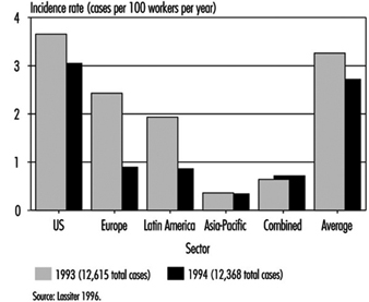
Figure 2. Distribution of incidence rates for Injuries and illnesses with days off from work by world sector 1993 and 1994
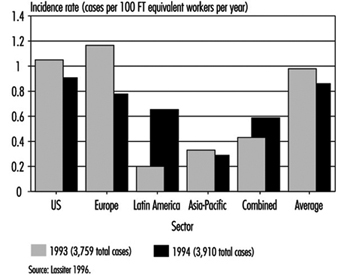
Figure 1 depicts work injury and illness incidence rates for the various world regions in the 1993-94 survey. Individual country rates have not been included to ensure confidentiality of those participating companies which were the sole sources of data for certain countries. Hence, for certain countries in the survey, data were reported for only a single facility. In several instances, companies combined all international data into a single statistic. These latter data are listed in figure 1 and figure 2 as “Combined”.
The annual incidence of work injuries and illnesses among all workers in the international survey was 3.3 cases per 100 employees (200,000 worker-hours) in 1993 and 2.7 in 1994. There were 12,615 cases reported for 1993 and 12,368 for 1994. The great majority of cases (12,130 in 1993) were derived from US companies. These cases were associated with approximately 387,000 workers in 1993 and 458,000 in 1994.
Figure 2 presents incidence rates for lost workday cases involving days away from work. The 1993 and 1994 incidence rates were based on approximately 4,000 lost workday cases for each of the 2 years in the international survey. The international/regional range in incidence rates for this statistic was the most narrow of those measured. The incidence of lost workday cases may represent the most comparable international statistics with respect to worker safety and health experience. The incidence rate for lost workdays (days away from work) was approximately 15.4 days away from work per 100 workers for each of the 2 years.
The only detailed data known to exist concerning case characteristics of semiconductor worker injuries and illnesses are those compiled annually in the US by the BLS, involving cases with lost workdays. The cases discussed here were identified by the BLS in their annual survey for the year 1993. Data obtained from these cases appear in figure 3, figure 4, figure 5 and figure 6. Each figure compares the lost workday case experience for the private sector, all manufacturing and semiconductor manufacturing.
Figure 3. Comparative incidence of lost workdays cases1 by type of event or exposure, 1993
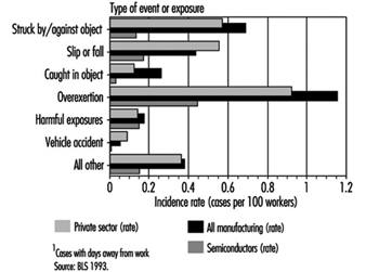
Figure 4. Comparative incidence of lost workday cases1 by source of injury or illness, 1993.
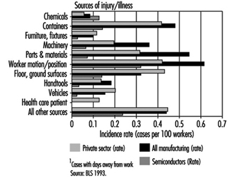
Figure 5. Comparative incidence of lost workday cases1 by nature of injury or illness, 1993.
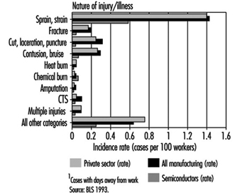
Figure 6. Comparative incidence of lost workday cases by part of body affected, 1993
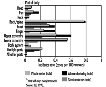
Figure 3 compares the lost workday case experience of US semiconductor workers in 1993 with the private sector and with all manufacturing with respect to type of event or exposure. The incidence rates for most categories in this figure were much less for semiconductor industry workers than for the private sector or all manufacturing. Cases involving overexertions among semiconductor workers were less than half the rate for all workers in the manufacturing sector. The harmful exposure category (primarily associated with exposures to chemical substances) was equivalent among all three groups.
Comparative distributions of lost workday cases according to source of injury or illness are presented in figure 4. Lost workday case incidence rates for semiconductor workers were less than those for the private sector and all manufacturing in all source categories except for cases associated with exposures to chemical substances.
Figure 5 compares lost workday case incidence rates associated with nature of injury or illness among the three groups. The rates for semiconductor workers were less than half of the rates for both the private sector and for all manufacturing in 1993. The incidence of chemical burns was slightly higher for semiconductor workers, but was very low for all three comparison groups. The incidence of carpal tunnel syndrome (CTS) among US semiconductor workers was less than half the rate for all manufacturing.
In figure 6, the distribution and incidence of cases involving days away from work is illustrated according to part of body affected. Although the incidence of cases involving body systems was low for all comparison groups, the rate for semiconductor workers was slightly elevated. All other body parts affected were much lower for semiconductor workers than for the other two comparison groups.
Epidemiological Studies of Semiconductor Workers
Concern for possible reproductive health consequences associated with employment in the semiconductor surfaced in 1983 when a female employee at the Digital Equipment Corporation’s semiconductor facility in Hudson, Massachusetts, indicated that she believed that an excess of miscarriages had occurred among employees in the facility’s cleanrooms. This allegation, coupled with an absence of internal data at the facility, led to an epidemiological study by the University of Massachusetts School of Public Health in Amherst (UMass). The study was begun in May of 1984 and completed in 1985 (Pastides et al. 1988).
An elevated risk of miscarriage was observed in both the photolithographic area and the diffusion area when compared to non-exposed workers in other areas of the facility. A relative risk of 1.75 was considered to be not statistically significant (p <0.05), although a 2.18 relative risk observed among workers in diffusion areas was significant. Publication of the UMass study led to concern throughout the semiconductor industry that a larger study was warranted to validate the observed findings and to determine their extent and possible causation.
The Semiconductor Industry Association (SIA) of the United States sponsored a larger study performed by the University of California at Davis (UC Davis) beginning in 1989. The UC Davis study was designed to test the hypothesis that semiconductor manufacturing was associated with an increased risk of miscarriage for female wafer fabrication employees. The study’s population was selected from among 14 companies which represented 42 production sites in 17 states. The highest number of sites (representing almost half of the employees in the study) was in California.
The UC Davis study consisted of three different components: a cross-sectional component (McCurdy et al. 1995; Pocekay et al. 1995); an historical cohort component (Schenker et al. 1995); and a prospective component (Eskenazi et al. 1995). Central to each of these studies was an exposure assessment (Hines et al. 1995; Hammond et al. 1995). The exposure assessment component assigned employees to a relative exposure group (i.e., high exposure, low exposure and so on).
In the historical component of the study, it was determined that the relative risk of fabrication workers, compared with non-fabrication workers, was 1.45 (i.e., 45% excess risk of miscarriage). The highest risk group identified in the historical component of the study were women who worked in photolithography or etching operations. Women performing etching operations experienced a relative risk of 2.15 (RR=2.15). In addition, a dose-response relationship was observed among women who worked with any photoresist or developer with respect to increased risk of miscarriage. These data supported a dose-response association for ethylene glycol ethers (EGE) but not for propylene glycol ethers (PGE).
Although an increased risk of miscarriage was observed among female wafer fabrication workers in the prospective component of the UC Davis study, the results were not statistically significant (p less than 0.05). A small number of pregnancies significantly reduced the power of the prospective component of the study. Analysis by exposure to chemical agent indicated an increased risk for those women who worked with ethylene glycol monoethyl ether, but was based on only 3 pregnancies. One important finding was the general support for, and not contradiction of, the findings of the historical component.
The cross-sectional component of the study noted an increase in upper respiratory symptoms primarily in the diffusion furnace and thin film groups of workers. An interesting finding was the apparent protective effects of various engineering controls related to ergonomics (e.g., footrests and the use of an adjustable chair to reduce back injuries).
Air measurements made in the wafer fabs found most solvent exposures were less than 1% of the permissible exposure limits (PEL) established by the US government.
A separate epidemiological study (Correa et al. 1996) was performed by the Johns Hopkins University (JHU), involving a group of IBM Corporation semiconductor employees in 1989. The overall miscarriage rate observed in the JHU study involving female cleanroom workers was 16.6%. The relative risk for miscarriage among female cleanroom workers with the highest potential exposure to ethylene glycol ethers was 2.8 (95% C.I. = 1.4-5.6).
Discussion of Reproductive Epidemiological Studies Involving Semiconductor Workers
The epidemiological studies were remarkable in the scope and similarity of results. These studies all produced similar findings. Each study documented an excess risk of spontaneous abortion (miscarriage) for female semiconductor wafer fabrication workers. Two of the studies (JHU and UC Davis) may indicate a causal association with exposures to ethylene-based glycol ethers. The UMass study found that the photo group (those exposed to glycol ether) had less risk than the diffusion group, which had no documented glycol ether exposure. While these studies indicate an increased risk of spontaneous abortions among wafer fabrication workers, the cause of such excess risk is unclear. The JHU study failed to document a significant role for glycol ethers, and the UC Davis study only marginally linked glycol ethers (through modelling of exposures and self-reported work practices) to reproductive effects. Little if any monitoring was performed in either study to determine exposures to glycol ethers. Following completion of these studies the semiconductor industry began switching from ethylene series glycol ethers to substitutes such as ethyl lactate and propylene series glycol ethers.
Conclusion
Based on the best available data concerning the annual incidence of work-related injuries and illnesses, semiconductor workers are at less risk than workers in other manufacturing sectors or throughout the private sector (including many non-manufacturing industries). On an international basis, it appears that work injury and illness statistical data associated with lost workday cases may be a fairly reliable indicator of the worldwide safety and health experience of semiconductor workers. The industry has sponsored several independent epidemiological studies in an attempt to find answers to questions of reproductive health consequences related to employment in the industry. Although a definitive association between observed miscarriages and exposures to ethylene-based glycol ethers was not established, the industry has begun to use alternative photoresist solvents.
Environmental and Public Health Issues
Industry Overview
The electronics industry, compared to other industries, has been viewed as “clean” in terms of its environmental impact. None the less, the chemicals used in the manufacture of electronic parts and components, and the waste generated, create significant environment issues that must be addressed on a global scale due to the size of the electronics industry. The wastes and by-products derived from the manufacture of printed wiring boards (PWBs), printed circuit boards (PCBs) and semiconductors are areas of interest that the electronic industry has vigorously pursued in terms of pollution prevention, treatment technology and recycling/reclamation techniques.
To a large degree, the incentive to control the environmental footprint of electronic processes has migrated from an environmental impetus to a financial domain. Due to the costs and liabilities associated with hazardous waste and emissions, the electronics industry has aggressively implemented and developed environmental controls that have greatly reduced the impact of its by-products and waste. In addition, the electronics industry has taken a proactive approach to incorporate environmental goals, tools and techniques into its environmentally conscious businesses. Examples of this proactive approach are the phase-out of CFCs and perfluorinated compounds and the development of “environmentally friendly” alternatives, as well as the emerging “design for the environment” approach to product development.
The manufacture of PWBs, PCBs and semiconductors requires the use of a variety of chemicals, specialized manufacturing techniques and equipment. Due to the hazards associated with these manufacturing processes, the proper management of chemical by-products, wastes and emissions is essential to assure the safety of the industry’s employees and the protection of the environment in the communities in which they reside.
Table 1, table 2 and table 3 present an outline of the key by-products and wastes that are generated in the manufacturing of PWBs, PCBs and semiconductors. In addition, the tables present the main types of environmental impact and the generally accepted means of mitigation and control of the waste stream. Primarily, the wastes that are generated affect industrial wastewater or the air, or become a solid waste.
Table 1. PWB waste generation and controls
|
Process steps |
Hazardous |
Environmental |
Controls1 |
|
Material |
None |
None |
None |
|
Stack and pin |
Heavy/precious metals |
Solid waste2 |
Recycle/reclaim |
|
Drilling |
Heavy/precious metals |
Solid waste2 |
Recycle/reclaim |
|
Deburr |
Heavy/precious metals |
Solid waste2 |
Recycle/reclaim |
|
Electroless |
Metals |
Wastewater |
Chemical precipitation |
|
Imaging |
Solvents |
Air |
Adsorption, condensation or |
|
Pattern plating |
Corrosives |
Wastewater/air |
pH neutralization/air scrubbing |
|
Strip, etch, strip |
Ammonia |
Air |
Air scrubbing (adsorption) |
|
Solder mask |
Corrosives |
Air |
Air scrubbing (adsorption) |
|
Solder coating |
Solvents |
Air |
Adsorption, condensation or |
|
Gold plating |
Corrosives |
Air |
Air scrubbing (adsorption) |
|
Component |
Solvents |
Air |
Adsorption condensation or |
1. Use of mitigation controls depends upon discharge limits in the specific location.
2. A solid waste is any discarded material regardless of its state.
Table 2. PCB waste generation and controls
|
Process steps |
Hazardous |
Environmental |
Controls |
|
Cleaning |
Metals (lead) |
Wastewater |
pH neutralization, chemical |
|
Solder paste |
Solder paste (lead/tin) |
Solid waste |
Recycle/reclaim |
|
Adhesive |
Epoxy glues |
Solid waste |
Incineration |
|
Component |
Plastic tapes, reels and tubes |
||
|
Adhesive cure and |
|||
|
Fluxing |
Solvent (IPA flux) |
Solid waste |
Recycle |
|
Wave soldering |
Metal (solder dross) |
Solid waste |
Recycle/reclaim |
|
Inspection and |
Metal |
Solid waste |
Recycle/reclaim |
|
Testing |
Scrapped populated |
Solid waste |
Recycle/reclaim |
|
Reworking and |
Metal (solder dross) |
Solid waste |
Recycle/reclaim |
|
Support |
Metal |
Solid waste |
Recycle/incineration |
Table 3. Semiconductor manufacturing waste generation and controls
|
Process steps |
Hazardous |
Environmental |
Controls |
|
Lithography/etching |
Solvents |
Solid waste |
Recycle/reclaim/incineration |
|
Oxidation |
Solvents |
Solid waste |
Recycle/reclaim/incineration |
|
Doping |
Poison gas (arsine, |
Air |
Substitution with liquid |
|
Chemical vapour deposition |
Metals Corrosives |
Solid waste |
Incineration |
|
Metallization |
Solvents |
Solid waste |
Incineration |
|
Assembly and testing |
Solvents |
Solid waste |
Recycle/reclaim/incineration |
|
Cleaning |
Corrosives |
Wastewater |
pH neutralization |
The following are generally accepted means of mitigating emissions in the PWB, PCB and semiconductor industries. The controls of choice will vary according to engineering capabilities, regulatory agency requirements and the specific constituents/concentrations of the waste stream.
Wastewater Control
Chemical precipitation
Chemical precipitation is generally used in the removal of particulate or soluble metals from wastewater effluents. Since metals do not naturally degrade and are toxic at low concentrations, their removal from industrial wastewater is essential. Metals can be removed from wastewater by chemical means since they are not very soluble in water; their solubilities depend upon the pH, metal concentration, type of metal and the presence of other ions. Typically, the waste stream requires pH adjustment to the proper level to precipitate out the metal. The addition of chemicals to wastewater in an effort to alter the physical state of dissolved and suspended solids is required. Lime, caustic and sulphide precipitation agents are commonly used. The precipitating agents facilitate the removal of dissolved and suspended metals by coagulation, sedimentation or entrapment within a precipitate.
A result of chemical precipitation of wastewater is the accumulation of sludge. Therefore, dewatering processes have been developed to reduce the weight of the sludge by means of centrifuges, filter presses, filters or drying beds. The resultant dewatered sludge can then be sent off for incineration or landfill.
pH neutralization
pH (the hydrogen-ion concentration or acidity) is an important quality parameter in industrial wastewater. Due to the adverse effects of pH extremes in natural waters and on sewage treatment operations, the pH of industrial wastewater must be adjusted prior to discharge from the manufacturing facility. Treatment occurs in a series of tanks that are monitored for the hydrogen-ion concentration of the wastewater effluent. Typically, hydrochloric or sulphuric acid is used as neutralizing corrosives, and sodium hydroxide is used as a neutralizing caustic. The neutralizing agent is metered into the wastewater effluent to adjust the pH of the discharge to its desired level.
Adjustment of pH is often required prior to the application of other wastewater treatment processes. Such processes include chemical precipitation, oxidation/reduction, activated carbon sorption, stripping and ion exchange.
Solid Waste Control
Materials are a solid waste if they are abandoned or discarded by being disposed of; burned or incinerated; or accumulated, stored or treated before or in lieu of being abandoned (US Code of Federal Regulation 40, Section 261.2). Hazardous waste generally exhibits one or more of the following characteristics: ignitability, corrosivity, reactivity, toxicity. Depending upon the characteristic of the hazardous material/waste, various means are used to control the substance. Incineration is a common treatment alternative for solvent and metal wastes generated during PWB, PCB and semiconductor manufacturing.
Incineration
Incineration (afterburner) or thermal destruction has become a popular option in handling ignitable and toxic wastes. In many instances, ignitable wastes (solvents) are used as a fuel source (fuel blending) for thermal and catalytic incinerators. Proper incineration of solvents and toxic wastes provides complete oxidation of the fuel and converts combustible material to carbon dioxide, water and ash, thereby leaving no liabilities associated with residual hazardous waste. The common types of incineration are thermal and catalytic incinerators. The selection of the type of incineration method is dependent upon the combustion temperature, fuel characteristics and residence time. Thermal incinerators operate at high temperatures and are widely used with halogenated compounds. Types of thermal incinerators include rotary kiln, liquid injection, fixed-hearth, fluidized bed and other advanced design incinerators.
Catalytic incinerators oxidize combustible materials (e.g., VOCs) by injecting a heated gas stream through a catalyst bed. The catalyst bed maximizes surface area, and by injecting a heated gas stream into the catalyst bed combustion can occur at a lower temperature than thermal incineration.
Air Emissions
Incineration is also used in control of air emissions. Absorption and adsorption are used as well.
Absorption
Air absorption is typically used in the scrubbing of corrosive air emissions, by passing the contaminant through and dissolving it in a non-volatile liquid (e.g., water). The effluent from the absorption process is typically discharged to a wastewater treatment system, where it undergoes pH adjustment.
Adsorption
Adsorption is the adherence (by means of physical or chemical forces) of a gas molecule to the surface of another substance, called an adsorbent. Typically, adsorption is used to extract solvents from an air emission source. Activated carbon, activated alumina or silica gel are commonly used adsorbents.
Recycling
Recyclable materials are used, reused or reclaimed as ingredients in an industrial process to make a product. Recycling of materials and waste provides environmental and economic means of effectively addressing specific types of waste streams, such as metals and solvents. Materials and wastes can be recycled in-house, or secondary markets may accept recyclable materials. The selection of recycling as an alternative for wastes must be evaluated against financial considerations, the regulatory framework and available technology to recycle the materials.
Future Direction
As the demand for pollution prevention increases and industry seeks cost-effective means to address chemical use and waste, the electronics industry must evaluate new techniques and technologies to improve the methods for hazardous-materials handling and waste generation. The end-of-pipe approach has been replaced by design for the environment techniques, where environmental issues are addressed over the full life cycle of a product, including: material conservation; efficient manufacturing operations; the use of more environmentally friendly materials; recycling, regeneration and reclamation of waste products; and a host of other techniques that will assure a smaller environmental impact for the electronics manufacturing industry. One example is the large amount of water that is used in the many rinsing and other processing steps in the microelectronics industry. In water-poor areas, this is forcing the industry to find alternatives. However, it is essential to make sure that the alternative (e.g., solvents) does not create additional environmental problems.
As an example of future directions in the PWB and PCB process, table 4 presents various alternatives for creating more environmentally sound practices and preventing pollution. Priority needs and approaches have been identified.
Table 4. Matrix of priority needs
|
Priority need (decreasing |
Approach |
Selected tasks |
|
More efficient use, |
Extend life of electrolytic and |
Research to extend baths. |
|
Reduce solid waste generated |
Develop and promote |
Develop infrastructure to |
|
Establish better supplier |
Promote supplier, |
Develop a model hazardous |
|
Minimize the impact of |
Reduce lead solder use when |
Change specifications to accept |
|
Use additive processes that |
Develop simplified, |
Collaborate on projects to |
|
Eliminate hole smear in PWB |
Develop no-smear resins or |
Investigate alternative |
|
Reduce water consumption |
Develop water use |
Modify specifications to reduce |
Source: MCC 1994.
" DISCLAIMER: The ILO does not take responsibility for content presented on this web portal that is presented in any language other than English, which is the language used for the initial production and peer-review of original content. Certain statistics have not been updated since the production of the 4th edition of the Encyclopaedia (1998)."