As an emerging industry, semiconductor manufacturing often has been viewed as the epitome of the high-technology workplace. Because of stringent manufacturing requirements associated with producing multiple layers of micron dimensional electronic circuitry on silicon wafers, the cleanroom environment has become synonymous with the workplace for this industry. Since certain of the hydride gases used in semiconductor manufacturing (e.g., arsine, phosphine) were recognized early as highly toxic chemicals, inhalation exposure control technology has always been an important component of wafer fabrication. Semiconductor workers are further isolated from the production process by wearing special clothing covering the whole body (e.g., gowns), hair covers, shoe covers and, frequently, facial masks (or even air-supplied breathing devices). From a practical standpoint, employer concerns for product purity have resulted, also, in worker exposure protection.
In addition to personal protective clothing, highly sophisticated systems of ventilation and chemical/gas air monitoring are used throughout the semiconductor industry to detect leaks of toxic chemical solvent vapours, acids and hydride gases at parts per million (ppm) or less. Although, from the historic viewpoint, the industry has experienced frequent worker evacuations from wafer fabrication rooms, based on real or suspected leaks of gases or solvents, such evacuation episodes have become rare events because of the lessons learned in design of ventilation systems, toxic gas/chemical handling and increasingly sophisticated air-monitoring systems with continuous air sampling. However, the increasing monetary value of individual silicon wafers (together with increasing wafer diameters), which can contain scores of individual microprocessors or memory devices, can place mental stress on workers who must manually manipulate containers of these wafers during manufacturing processes. Evidence of such stress was obtained during a study of semiconductor workers (Hammond et al. 1995; Hines et al. 1995; McCurdy et al. 1995).
The semiconductor industry had its beginnings in the United States, which has the highest number of semiconductor industry workers (approximately 225,000 in 1994) of any country (BLS 1995). However, obtaining valid international employment estimates for this industry is difficult because of the inclusion of semiconductor workers with “electrical/electronic equipment manufacturing” workers in most nations’ statistics. Because of the highly stringent engineering controls required for semiconductor device manufacturing, it is most probable that semiconductor workplaces (i.e., cleanrooms) are comparable, in most respects, throughout the world. This understanding, coupled with US government requirements for recording all significant work-related injuries and illnesses among US workers, makes the work injury and illness experience of US semiconductor workers a highly relevant issue on both a national and international scale. Simply stated, at this time there are few international sources of relevant information and data concerning semiconductor worker safety and health experience, other than those from the Annual Survey of Occupational Injuries and Illnesses by the US Bureau of Labor Statistics (BLS).
In the United States, which has collected work injury and illness data on all industries since 1972, the frequency of work-related injuries and illnesses among semiconductor workers has been among the lowest of all manufacturing industries. However, concerns have been voiced that more subtle health effects may be present among semiconductor workers (LaDou 1986), although such effects have not been documented.
Several symposia have been held concerning control technology assessment in the semiconductor industry, with several of the symposia papers dealing with environmental and worker safety and health issues (ACGIH 1989, 1993).
A limited quantity of work injury and illness data for the international semiconductor manufacturing community was derived via a special survey performed in 1995, involving cases reported for the years 1993 and 1994. These survey data are summarized below.
Work Injuries and Illness among Semiconductor Workers
With respect to international statistical data associated with work injuries and illnesses among semiconductor workers, the only comparable data appear to be those derived from a survey of multi-national semiconductor manufacturing operations performed in 1995 (Lassiter 1996). The data collected in this survey involved the international operations of US-based semiconductor manufacturers for the years 1993-94. Some of the data from the survey included operations other than semiconductor manufacturing (e.g., computer and disk drive manufacturing), although all participating companies were involved in the electronics industry. The results of this survey are presented in figure 1 and figure 2, which include data from the Asia-Pacific region, Europe, Latin America and the United States. Each case involved a work-related injury or illness which required medical treatment or work loss or restriction. All incidence rates in the figures have been calculated as numbers of cases (or lost workdays) per 200,000 worker-hours per year. If total worker-hours was not available, average annual employment estimates were used. The 200,000 worker-hours denominator is equal to 100 full-time equivalent workers per year (assuming 2,000 work hours per worker per year).
Figure 1. Distribution of incidence rates for work injuries and illnesses by world sector, 1993 and 1994.
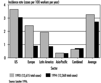
Figure 2. Distribution of incidence rates for Injuries and illnesses with days off from work by world sector 1993 and 1994
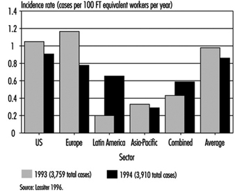
Figure 1 depicts work injury and illness incidence rates for the various world regions in the 1993-94 survey. Individual country rates have not been included to ensure confidentiality of those participating companies which were the sole sources of data for certain countries. Hence, for certain countries in the survey, data were reported for only a single facility. In several instances, companies combined all international data into a single statistic. These latter data are listed in figure 1 and figure 2 as “Combined”.
The annual incidence of work injuries and illnesses among all workers in the international survey was 3.3 cases per 100 employees (200,000 worker-hours) in 1993 and 2.7 in 1994. There were 12,615 cases reported for 1993 and 12,368 for 1994. The great majority of cases (12,130 in 1993) were derived from US companies. These cases were associated with approximately 387,000 workers in 1993 and 458,000 in 1994.
Figure 2 presents incidence rates for lost workday cases involving days away from work. The 1993 and 1994 incidence rates were based on approximately 4,000 lost workday cases for each of the 2 years in the international survey. The international/regional range in incidence rates for this statistic was the most narrow of those measured. The incidence of lost workday cases may represent the most comparable international statistics with respect to worker safety and health experience. The incidence rate for lost workdays (days away from work) was approximately 15.4 days away from work per 100 workers for each of the 2 years.
The only detailed data known to exist concerning case characteristics of semiconductor worker injuries and illnesses are those compiled annually in the US by the BLS, involving cases with lost workdays. The cases discussed here were identified by the BLS in their annual survey for the year 1993. Data obtained from these cases appear in figure 3, figure 4, figure 5 and figure 6. Each figure compares the lost workday case experience for the private sector, all manufacturing and semiconductor manufacturing.
Figure 3. Comparative incidence of lost workdays cases1 by type of event or exposure, 1993
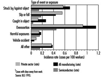
Figure 4. Comparative incidence of lost workday cases1 by source of injury or illness, 1993.
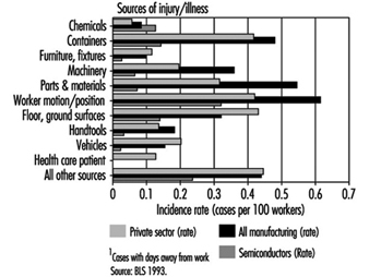
Figure 5. Comparative incidence of lost workday cases1 by nature of injury or illness, 1993.
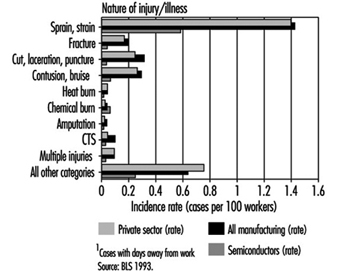
Figure 6. Comparative incidence of lost workday cases by part of body affected, 1993
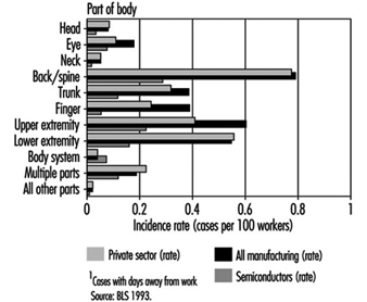
Figure 3 compares the lost workday case experience of US semiconductor workers in 1993 with the private sector and with all manufacturing with respect to type of event or exposure. The incidence rates for most categories in this figure were much less for semiconductor industry workers than for the private sector or all manufacturing. Cases involving overexertions among semiconductor workers were less than half the rate for all workers in the manufacturing sector. The harmful exposure category (primarily associated with exposures to chemical substances) was equivalent among all three groups.
Comparative distributions of lost workday cases according to source of injury or illness are presented in figure 4. Lost workday case incidence rates for semiconductor workers were less than those for the private sector and all manufacturing in all source categories except for cases associated with exposures to chemical substances.
Figure 5 compares lost workday case incidence rates associated with nature of injury or illness among the three groups. The rates for semiconductor workers were less than half of the rates for both the private sector and for all manufacturing in 1993. The incidence of chemical burns was slightly higher for semiconductor workers, but was very low for all three comparison groups. The incidence of carpal tunnel syndrome (CTS) among US semiconductor workers was less than half the rate for all manufacturing.
In figure 6, the distribution and incidence of cases involving days away from work is illustrated according to part of body affected. Although the incidence of cases involving body systems was low for all comparison groups, the rate for semiconductor workers was slightly elevated. All other body parts affected were much lower for semiconductor workers than for the other two comparison groups.
Epidemiological Studies of Semiconductor Workers
Concern for possible reproductive health consequences associated with employment in the semiconductor surfaced in 1983 when a female employee at the Digital Equipment Corporation’s semiconductor facility in Hudson, Massachusetts, indicated that she believed that an excess of miscarriages had occurred among employees in the facility’s cleanrooms. This allegation, coupled with an absence of internal data at the facility, led to an epidemiological study by the University of Massachusetts School of Public Health in Amherst (UMass). The study was begun in May of 1984 and completed in 1985 (Pastides et al. 1988).
An elevated risk of miscarriage was observed in both the photolithographic area and the diffusion area when compared to non-exposed workers in other areas of the facility. A relative risk of 1.75 was considered to be not statistically significant (p <0.05), although a 2.18 relative risk observed among workers in diffusion areas was significant. Publication of the UMass study led to concern throughout the semiconductor industry that a larger study was warranted to validate the observed findings and to determine their extent and possible causation.
The Semiconductor Industry Association (SIA) of the United States sponsored a larger study performed by the University of California at Davis (UC Davis) beginning in 1989. The UC Davis study was designed to test the hypothesis that semiconductor manufacturing was associated with an increased risk of miscarriage for female wafer fabrication employees. The study’s population was selected from among 14 companies which represented 42 production sites in 17 states. The highest number of sites (representing almost half of the employees in the study) was in California.
The UC Davis study consisted of three different components: a cross-sectional component (McCurdy et al. 1995; Pocekay et al. 1995); an historical cohort component (Schenker et al. 1995); and a prospective component (Eskenazi et al. 1995). Central to each of these studies was an exposure assessment (Hines et al. 1995; Hammond et al. 1995). The exposure assessment component assigned employees to a relative exposure group (i.e., high exposure, low exposure and so on).
In the historical component of the study, it was determined that the relative risk of fabrication workers, compared with non-fabrication workers, was 1.45 (i.e., 45% excess risk of miscarriage). The highest risk group identified in the historical component of the study were women who worked in photolithography or etching operations. Women performing etching operations experienced a relative risk of 2.15 (RR=2.15). In addition, a dose-response relationship was observed among women who worked with any photoresist or developer with respect to increased risk of miscarriage. These data supported a dose-response association for ethylene glycol ethers (EGE) but not for propylene glycol ethers (PGE).
Although an increased risk of miscarriage was observed among female wafer fabrication workers in the prospective component of the UC Davis study, the results were not statistically significant (p less than 0.05). A small number of pregnancies significantly reduced the power of the prospective component of the study. Analysis by exposure to chemical agent indicated an increased risk for those women who worked with ethylene glycol monoethyl ether, but was based on only 3 pregnancies. One important finding was the general support for, and not contradiction of, the findings of the historical component.
The cross-sectional component of the study noted an increase in upper respiratory symptoms primarily in the diffusion furnace and thin film groups of workers. An interesting finding was the apparent protective effects of various engineering controls related to ergonomics (e.g., footrests and the use of an adjustable chair to reduce back injuries).
Air measurements made in the wafer fabs found most solvent exposures were less than 1% of the permissible exposure limits (PEL) established by the US government.
A separate epidemiological study (Correa et al. 1996) was performed by the Johns Hopkins University (JHU), involving a group of IBM Corporation semiconductor employees in 1989. The overall miscarriage rate observed in the JHU study involving female cleanroom workers was 16.6%. The relative risk for miscarriage among female cleanroom workers with the highest potential exposure to ethylene glycol ethers was 2.8 (95% C.I. = 1.4-5.6).
Discussion of Reproductive Epidemiological Studies Involving Semiconductor Workers
The epidemiological studies were remarkable in the scope and similarity of results. These studies all produced similar findings. Each study documented an excess risk of spontaneous abortion (miscarriage) for female semiconductor wafer fabrication workers. Two of the studies (JHU and UC Davis) may indicate a causal association with exposures to ethylene-based glycol ethers. The UMass study found that the photo group (those exposed to glycol ether) had less risk than the diffusion group, which had no documented glycol ether exposure. While these studies indicate an increased risk of spontaneous abortions among wafer fabrication workers, the cause of such excess risk is unclear. The JHU study failed to document a significant role for glycol ethers, and the UC Davis study only marginally linked glycol ethers (through modelling of exposures and self-reported work practices) to reproductive effects. Little if any monitoring was performed in either study to determine exposures to glycol ethers. Following completion of these studies the semiconductor industry began switching from ethylene series glycol ethers to substitutes such as ethyl lactate and propylene series glycol ethers.
Conclusion
Based on the best available data concerning the annual incidence of work-related injuries and illnesses, semiconductor workers are at less risk than workers in other manufacturing sectors or throughout the private sector (including many non-manufacturing industries). On an international basis, it appears that work injury and illness statistical data associated with lost workday cases may be a fairly reliable indicator of the worldwide safety and health experience of semiconductor workers. The industry has sponsored several independent epidemiological studies in an attempt to find answers to questions of reproductive health consequences related to employment in the industry. Although a definitive association between observed miscarriages and exposures to ethylene-based glycol ethers was not established, the industry has begun to use alternative photoresist solvents.